Unlike the ideal models, real operational amplifiers have imperfections which can cause errors in practical applications. This article is going to briefly discuss these imperfections and some compensation methods to optimize op-amp implementation.
- Common-Mode Gain
- Offset Voltage
- Bias Current
- Drift
- Frequency response
Common-Mode Gain
An op-amp amplifies the voltage difference between its two inputs. Thus, if there is no potential difference between the inputs, then there is no voltage to be amplified and there will be no change in the output voltage for any arbitrary common-mode input. Ideal op-amps supposedly follow this theoretical common-mode voltage gain of zero. However, this condition is not easily achieved for real op-amps and common-mode voltages will have some effects on the output.
The common-mode rejection ratio (CMRR) measures the performance of real op-amps in this regard. CMRR is the ratio of an op-amp’s differential voltage gain to its common-mode voltage gain. While ideal op-amps have infinite CMRRs, real op-amps have high but still measurable CMRRs.
In differential op-amp circuits such as instrumentation amplifiers, common-mode gain can be caused by an imbalance of resistor values. Consider the circuit below:

With inputs shorted, a common-mode voltage can be imposed and with a perfectly balanced circuit, no change in output voltage is expected. Imposing a common-mode voltage by introducing a resistor imbalance (for example, setting the value of R5 to 10.5kΩ while maintaining the rest at 10kΩ) results in a significant change in the output. To avoid this, it is necessary to balance all resistor values. To avoid common-mode gain introduced by imperfection in op-amps in a balanced circuit, adjust the value of at least one of the four resistors connected to the final op-amp to compensate for the gain.
For circuits where the op-amp is being used with negative feedback, the change in the output due to the effect of the common-mode gain would be corrected as negative feedback. With high CMRRs (differential gain being much greater than common-mode gain), the system will be back to equilibrium even when sudden changes in the common-mode input occur.
Offset Voltage
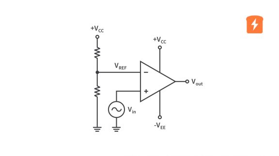
When the voltage difference between the two inputs is zero yet the output voltage is not zero (as what commonly happens for real op-amps), this deviation from the expected value of zero is called offset. For the op-amp below, the output is saturated at 14.7V due to the saturation limitations of this particular op-amp. The voltage offset present at the output cannot be determined as it is driving the output to a saturated point.


Offset voltage is typically quantified in terms of the input voltage differential producing the effect. Assuming that the op-amp has no offset, a small voltage applied (in series) to one of the inputs must be causing the offset. Since op-amp differential gains are very high, a small input offset voltage can account for saturated outputs.
To compensate for offset voltage, manufacturers make provisions to trim the offset of their op-amps. Usually, trim potentiometers can be connected to reserved terminals (see op-amp below), creating offset null connection points.

Different op-amp models may have offset null connections in different pin locations so it is imperative to refer to the manufacturer’s specifications for proper configuration.
Bias Current
Op-amps have bias currents to properly bias their internal circuits. These currents in most cases of op amp circuit analysis are considered negligible. However, bias currents might cause problems in some applications.
For example in the comparator circuits below, voltage generated by the thermocouple drives the op-amp either positive or negative. A not so apparent problem is that the wire loop does not provide a path for the input bias currents because both bias currents are going in the same direction. Grounding one of the inputs makes the circuit work as it provides a path for both currents.


A conductive path from one input to the other is not enough; both bias currents should have paths to flow to either one of the supply rails or to ground. Bias current flowing through resistances can also cause offset voltages. Assuming that the bias currents are equal, an equivalent resistance can be connected in series with the other op-amp input as a compensating resistor. To form proper paths for bias, feedback and load currents, a ground reference on a terminal of the power supply is essential.
Drift
As semiconductor devices, op-amps are sensitive to temperature. Op-amp drift pertains to any slight effect in device performance or behavior caused by changes in operating temperature. Op-amps have drift parameters in the manufacturer’s data sheet and minimizing drift effects may be taken into account in inspecting op-amp specifications. Another way to minimize drift is to keep the operating temperature stable. This can be achieved by utilizing inevitably costly equipment in laboratories for high accuracy applications.
Frequency Response
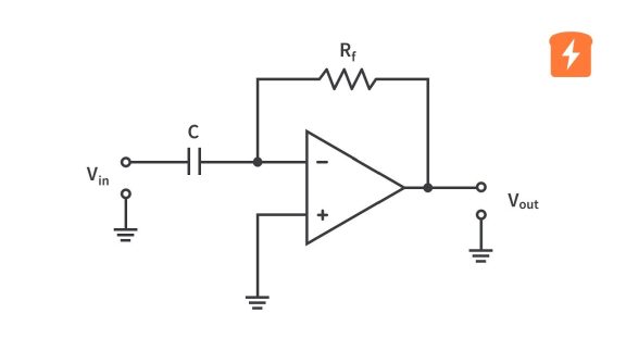
Op-amp circuits are susceptible to feedback oscillation when the output self-oscillates (feeds back to the op-amp to be amplified again) due to the high differential voltage gain. For some op-amps connected as a voltage follower with minimal connections (supply, two inputs and output), the output will self-oscillate due to the high gain regardless of the input voltage. To counteract this, the op-amp will have specific terminals where a small compensation capacitor can be connected. This decreases the AC gain and prevents undesirable oscillations by introducing a high-impedance path for negative feedback within the op-amp circuitry. For high-frequency signal amplification, compensation capacitors may not be necessary. However, they are essential for DC or low-frequency signals.
Some op-amps have built-in compensators but the capacitance inside the op-amp causes the differential voltage gain to decrease with increasing input frequency. As a result, the op-amp is less effective in higher frequencies.
During the circuit design process, it must be taken into account if sufficient and consistent op-amp performance is to be maintained within the range of signal frequencies required. Op-amp frequency response curves published by the manufacturers are the references for determining limits of effective operation.
Conclusion
Errors caused by real op-amp imperfections can be unacceptable in certain applications. In such cases, imperfections must be compensated for by the choice of op-amp, slight circuit adjustments or other more advanced laboratory equipment. Thorough perusal of op-amp specifications, balancing the circuit and forming proper paths for bias currents are some key measures to ensure desirable op-amp and/or circuit function.


