Create your own simple oscilloscope with ADC and 1602 LCD Using MCC | Embedded C Programming - Part 29
Published
Hi there! Once we have started learning the analog modules of the PIC18F14K50 MCU, we will discuss everything related to it accordingly.
In the previous tutorial, we started with the analog comparator, and this one will be devoted to the analog-to-digital (ADC) module. As its name suggests, this module converts the input analog signal into digital code, which the MCU program can use. With the PIC10F200 MCU, we had to add some external components and some calculations to measure the input voltage, and in PIC18F14K50, everything is done by the hardware ADC module, and we get the final result from it.
The task for the current tutorial will not be easy. We will create an oscilloscope showing the input signal’s waveform in character 1602 LCD. Yes, that’s not a joke! We can do this. For sure, the resolution of this oscilloscope will be very low - just 16 pixels in height and 24 pixels in width, so this project doesn’t pretend to be a practical device but more like a demonstration of what can be done if you have enough imagination (and don’t have a normal display 🙂).
In this tutorial, we will use only one new module - ADC. But it has a lot of parameters and settings, so its consideration will take quite a lot of time.
ADC Module
Before you proceed with the following reading, please familiarize yourself with ADC operation theory if you don’t know it.
So, the ADC in the PIC18F14K50 MCU has a 10-bit resolution, meaning that the input signal converts into the digital value from 0 to 1023. The PIC18F14K50 has a single ADC unit with 11 inputs - 9 external and 2 internal. These inputs all come to the analog multiplexer, which connects one of them to the sample-and-hold circuit of the ADC. The 9 external inputs are merged with the IO pins, and the internal ones are the output of the fixed and programmable reference voltage sources.
From the output of the sample-and-hold circuit, the signal goes to the converter’s input. ADC of the PIC18F14K50 MCU is the successive approximation register (SAR) type. This type has a relatively high speed and a mediocre resolution compared to other types. The result of the conversion is saved in two registers - ADRESL and ARDRESH, which are the lower and upper bytes of the result, respectively.
Speaking of the result, it can be aligned right or left. Alignment right means that the LSB of the conversion result will match with the LSB of the ADRESL register, and the upper six bits of the ADRESH register will be unused. Alignment left is the opposite - the MSB of the conversion result will match with the MSB of the ADRESH register, and the lower six bits of the ADRESL register will be unused. The latter option can be used if you don’t need high accuracy. In this case, you can only read the ADRESH register, containing the upper 8 bits of the conversion result.
The reference voltage of the ADC is selectable. The positive reference voltage can be chosen between the supply voltage VDD, external reference voltage applied to the dedicated pin VREF+, or internal fixed reference voltage source (FRV). The negative reference voltage can be chosen between the ground level voltage (VSS) or external reference voltage applied to the dedicated pin (VREF-).
The ADC can generate the interrupt on completion of the conversion, which can be used to wake up the MCU from sleep mode.
That’s all the general information about the ADC module. The rest of it I will provide when describing the MCC-based configuration of it.
If you want to know more about the ADC module, please refer to chapter 17 of the PIC18F14K50 data sheet.
Schematic Diagram
The schematic diagram is shown in Figure 1.

This schematic diagram is very similar to the one presented in tutorial 25 but even simpler: it consists of the PIC18F14K50 MCU (DD1) and 1602 character LCD (X2), which are connected in the same way as there. There are no other external components, though - only the analog input AIN, whose positive output of no more than the VDD voltage goes to the pin RA4, which is merged with the analog input AIN3, and the negative output is connected to the ground (don’t mix them up!)
I will explain the algorithm for showing the graphic information on the character display later when we consider the program code. And for now, that’s everything about the device schematic diagram so we can proceed to the next step.
Configuration of the Project using MCC
Let’s create a new project now. I’ve called it “Oscilloscope_MCC,” but you can give it any name you want.
We must configure Timer3 and ADC modules with the MCC in this project. The timer will be needed to start the ADC conversion in the specified time intervals, so the sampling will always happen with a constant period.
Let’s create a new project, run the MCC plugin, and change the MCU package. Open the System Module page, set the Internal Clock as 8MHz_HF, and set the “PLL Enabled” checkbox. Also, don’t forget to remove the check from the “Low-voltage programming enable” field (Figure 2).

Then we need to go to the Device resources tab on the left part of the screen, expand the drop-down list “Timer," and click on the green plus at “TMR3” (Figure3).

Then we need to expand the “ADC” list and add the “ADC” position (Figure 4).

After that, your Resource Management window should look like in Figure 5.

Now, let’s open the TMR3 window and configure the Timer3 module according to Figure 6.

You can read about the Timer3 configuration in more detail in tutorial 25. Here we only need to enable the timer overflow interrupt and specify the timer period as 166.66 us. As you can see, this period can’t be set due to lack of resolution, so the actual period will be 166.625 us, which is very close to the desired one.
Here Timer3 will be used as a timer that generates the interrupts in a defined interval. When these interrupts happen, we will start the AD conversion. So using the timer, we can be sure that the measurements of the input analog signal will be done with a constant period.
Now we can take a break regarding the configuration. Clear your mind for further explanation of what outcome we intend to see.
The 1602 LCD looks like in Figure 7.

Each dark rectangle is 5x8 dots, and the distance between the rectangles is one dot. As I told you in Tutorial 19, apart from the predefined characters, the HD44780 driver also has the CGRAM area, which can be used to generate our own characters. We will use this area to display the input signal’s waveform. Unfortunately, the number of manual characters is just 8, so we can’t spread the graphical image on the entire display. We can make either a thin graph of one line, 8 characters width, or a tall graph of two lines but only 4 character width. I used the second option so that the whole graph will occupy just the area of 2x4 characters.
Also, not to have the step in the graph between the characters, I decided that the space between them would also be considered an active area. So, in this case, the resolution of the graph area in pixels will be 23 x 17 (4 x 5 pixels + 3 empty lines and 2 x 8 pixels + 1 empty line).
Then it would be good if one character corresponds to some round number in a horizontal direction, for example, 1 ms. So you can use the spaces as grid lines. As the distance between the empty spaces is 6 dots, to get the resolution of 1 ms/div, we need to read the input signal every 1 / 6 = 0.16667 ms, or 166.67 us. The closest value that can be achieved by the timer using the maximum CPU frequency is 16.625 us - the value we have set in Figure 6.
As for the vertical resolution, we will use just 16 bits of 17. There are two reasons for this. First, it simplifies the calculations, as we will be able to use a 16-bit value, and to deal with 17 bits, we would need to switch to 32-bit values. And secondly, I usually use the supply voltage provided by the PICKit as 3.25V. And if we divide 3.25 by 16, we will get a vertical resolution of almost precisely 200 mV/pixel, or 1.6V/div. If we divide 3.25 by 17, the resolution will be 191 mV which is also not bad but still worse than the even 200 mV/pixels we get when using 16 pixels.
Now, let’s return to the MCU configuration and switch to the ADC tab and configure the ADC module (Figure 8).

Let’s see what options the ADC module has:
- Sets the clock source of the ADC module. The available ranges are from FOSC/2 to FOSC/64, and the dedicated internal oscillator FRC with a nominal frequency of 600 kHz. In our case FOSC is set as 32 MHz (see Figure 2), so the ADC module frequency will be fADC = 32 / 32 = 1 MHz. For the ADC module, there is such a parameter as TAD which is the period of one ADC clock tick. TAD = 1 / fADC. In our case, TAD = 1 / 1 MHz = 1 us. There are strict requirements for the ADC frequency - it should be selected so that the TAD lies between 0.7us and 4 us. And the selected value fits into this range perfectly.
- Acquisition time is how long the AD sample-and-hold circuit holds the capacitor connected to the input channel after the GO/DONE bit is set before the conversion begins. This time is measured in the number of TADs in the 0 to 20 TAD range. Selecting the proper acquisition time is a challenging task and requires many calculations based on the parameters of the external circuit and the environment temperature. I will not provide them here, but you can read them in chapter 17.3 of the PIC18F14K50 data sheet. The sampling period of 16.625 us (Timer3 period) will be enough for both auto acquisition and conversion, so we don’t need to add more acquisition time.
- Information about the ADC timing parameters. You can see here that it confirms our calculation of the TAD value. The conversion time always takes 11.5 TAD; also, it takes 2 TAD for the capacitor discharge, so even if the acquisition time is 0, the max sampling frequency is 1 / (11.5 + 2) us = 74.0741 kHz, which we also see in Figure 7.
- Enables the “ADC Conversion Complete” interrupt. We will use it to know when the newly converted data is ready, so we mark this checkbox.
- Allows to align the conversion result right or left. In the first case, the conversion result occupies the lower 10 bits of the 16-bit value leaving the higher 6 bits unused. In the second case, the conversion result occupies the upper 10 bits of the 16-bit value leaving the lower 6 bits unused. Right alignment is more natural, so we will select this option.
- Selects the positive reference voltage source. It can be supplied either internally by the VDD (default option in MCC), internally by the fixed reference voltage module (FRV), or externally by the VREF+ pin. We will leave the default option; in this case we can reach the rail-to-rail sensitivity of the ADC.
- Selects the negative reference voltage source. It can be supplied either internally by the VSS (default option in MCC), or externally by the VREF- pin. We will leave the default option here as well.
- Shows the selected channels of the ADC module. The internal channels (FRV and DAC) are always available, and the external channels are selected in the Pin Manager, which we will consider right now.
So let’s switch to the Pin Module and Pin Manager and configure all required pins according to the schematic diagram (Figure 9).

As you can see, apart from the LCD pins D4, D5, D6, D7, RS, and E (which are the same as in Tutorial 23), we have one more pin - channel_AN3. To configure it as the input of the ADC, we need to right-click on the RA4 pin in the Pin Manager and select the “ADC | ANx | input” option (Figure 10).

As you see in Figure 8, the RA4 pin has the ADC function and the Analog type. You must not remove the check from the “Analog” checkbox if you want the pin to work in the analog mode.
Finally, let’s switch to the Interrupt Module tab and enable the TMR3 and ADC interrupts (Figure 11).

There is no need to enable the priorities of the interrupts as they are not challenging.
Now everything is configured, and we can click the “Generate” button and switch to code writing.
Program Code Description
The same as in tutorial 25; we will need to copy and paste the “lcd_1602_mcc.h” and “lcd_1602_mcc.c”. One can take them from tutorial 25 in the same way I showed you. After all, your project should look like in Figure 12.

If you compare the schematic diagrams (Figure 1) in the current tutorial and tutorial 25, you will notice that the connection of the display is equal, so if you took the LCD-related files from it, you don’t need to make any changes to it. And if you copied them from one of the previous tutorials, please remember to change the pin assignment; otherwise, your display won’t work properly.
Now, consider the “main.c” file and write the following code.
#include "mcc_generated_files/mcc.h"
#include "lcd_1602_mcc.h"

#define THRESHOLD 256       	//Synchronization threshold

volatile uint8_t count;     	//Counter of the AD conversions
volatile uint16_t adc_data[50]; //Array to store the AD conversions

void refresh_display (void) 	//Function to refresh the display view
{
    uint8_t min, max;   //Minimum and maximum values of the neighbor conversions
    uint8_t character[2][8];	//Array for the display character generator
    uint16_t display_buffer[24];//Display's canvas area
    uint8_t start_index = 25;   //Start index of the adc_data array
    uint32_t max_v = adc_data[0];//Maximum voltage
    uint32_t min_v = adc_data[0];//Minimum voltage
    uint32_t avg_v = adc_data[0];//Average voltage
    for (uint8_t i = 1; i < 50; i ++)//Loop throughout the whole adc_data array
    {
        if (adc_data[i] > max_v)	//If the current adc_data element is greater than max_v
            max_v = adc_data[i];	//then assign the max_v as the current adc_data element
        if (adc_data[i] < min_v)	//If the current adc_data element is smaller than min_v
            min_v = adc_data[i];	//then assign the min_v as the current adc_data element
        avg_v += adc_data[i];   	//Accumulate the adc_data array values
    }
    avg_v /= 50;                	//Calculate the average voltage
    min_v = (min_v * 325) / 10240;  //Convert the minimum voltage into 0.1V
    max_v = (max_v * 325) / 10240;  //Convert the maximum voltage into 0.1V
    avg_v = (avg_v * 325) / 10240;  //Convert the average voltage into 0.1V
    for (uint8_t i = 0; i < 25; i ++)//Loop to find the start element in the adc_data array
    {
        if ((adc_data[i] < THRESHOLD) && (adc_data[i + 1] >= THRESHOLD))//If the current element is smaller than THRESHOLD and the next element is greater than THRESHOLD
        {
            start_index = i;    	//then save the index of the current element
            break;              	//and leave the loop
        }
    }
    for (uint8_t i = 0; i < 24; i ++)   //Loop to fill the display's canvas buffer
    {
        min = (adc_data[i + start_index] >= adc_data[i + start_index + 1]) ? adc_data[i + start_index + 1] >> 6 : adc_data[i + start_index] >> 6;// Select the minimum value between the neighbor ones
        max = (adc_data[i + start_index] >= adc_data[i + start_index + 1]) ? adc_data[i + start_index] >> 6 : adc_data[i + start_index + 1] >> 6;// Select the maximum value between the neighbor ones
        display_buffer[i] = 0;      	//Clear the current display_buffer element
        for (uint8_t j = min; j <= max; j ++)   //Loop from the min to max values
        {
            display_buffer[i] += 1 << j;	//Add the 1 at the corresponding position
        }
    }
    for (uint8_t k = 0; k < 4; k ++)//Loop to generate the characters for the display
    {
        for (uint8_t i = 0; i < 8; i ++)//Loop to form 8 lines of the character generator
        {
            character[0][7 - i] = 0;    	//Clear the current character[0] element
            character[1][7 - i] = 0;    	//Clear the current character[1] element
            for (uint8_t j = 0; j < 5; j ++)//Loop to convert the display_buffer into the character
            {
                character[0][7 - i] += ((display_buffer[4 - j + k * 6] & (1 << (i + 9))) >> (i + 9)) << j;//Convert the upper line
                character[1][7 - i] += ((display_buffer[4 - j + k * 6] & (1 << i)) >> i) << j;  //Convert the lower line
            }
        }
        lcd_create_char(k, character[0]);   //Create the character of the upper line
        lcd_create_char(k + 4, character[1]);//Create the character of the lower line
    }
    lcd_set_cursor(1, 1);       //Set the cursor at the first position of the upper line
    for (uint8_t i = 0; i < 4; i ++)	//Loop to send four generated characters
        lcd_data(i);                	//to the upper line

    lcd_set_cursor(1, 2);  //Set the cursor at the first position of the lower line
    for (uint8_t i = 4; i < 8; i ++)	//Loop to send four generated characters
        lcd_data(i);                	//to the lower line

    lcd_set_cursor (6, 1);   //Set the cursor at the sixth position of the upper line
    lcd_write_number(min_v, 1);     	//Write the minimum voltage
    lcd_write_string("V<U<");       	//Write the text
    lcd_write_number(max_v, 1);     	//Write the maximum voltage
    lcd_write_string("V	");      	//Write the text
    lcd_set_cursor (6, 2);    //Set the cursor at the sixth position of the lower line
    lcd_write_string("AVG:");       	//Write the text
    lcd_write_number(avg_v, 1);     	//Write the average voltage
    lcd_write_string("V	");      	//Write the text
}

void timer3_isr_handler (void)      	//Timer3 overflow interrupt subroutine
{
    ADC_StartConversion();          	//Start ADC conversion
}

void adc_isr_handler (void)      //ADC conversion complete interrupt subroutine
{
    adc_data[count] = ADC_GetConversionResult();//Read the ADC conversion result
    count ++;                       	//Increment the count value
    if (count >= 50)                	//If count exceeds the adc_data array size
    {
        INTERRUPT_PeripheralInterruptDisable();//Disable all peripheral interrupts
        refresh_display();          	//Refresh the display
        count = 0;                  	//Reset the count value
        __delay_ms(500);            	//Perform 500 ms delay
        INTERRUPT_PeripheralInterruptEnable();//Enable peripheral interrupts
    }
}

void main(void)
{
    SYSTEM_Initialize();            	// Initialize the device

    TMR3_SetInterruptHandler (timer3_isr_handler);//Set Timer3 interrupt handler
    ADC_SelectChannel(channel_AN3); 	//Select the AD conversion channel
    ADC_SetInterruptHandler (adc_isr_handler);  //Set ADC interrupt handler

    lcd_init(0, 0);     	//Initialize the LCD without cursor and blinking

    INTERRUPT_GlobalInterruptEnable();  //Enable global interrupts
    INTERRUPT_PeripheralInterruptEnable();  //Enable peripheral interrupts

    while (1);
}
This program is one of the most extensive and most likely the most difficult among the others we wrote in previous tutorials.
In line 1, we, as usual, include the “mcc_generated_files/mcc.h” file to be able to use the MCC-generated variables, functions, and macros. In line 3, we include the “lcd_1602_mcc.h” file, which consists of the 1602 LCD-related functions.
In line 4, we define the THRESHOLD macro, which specifies the synchronization threshold for the displayed graph. I will explain this part later, and now remember that we have such a value.
In lines 6 and 7, we declare two global variables: count (line 7), which is the counter of the ADC measurements, and the array of 50 16-bit elements adc_data (line 8) into which the consequent ADC measurements will be stored. The size of the array also is not random and will be explained in a proper time.
In lines 9-80, there is the function refresh_display in which all the calculations are done. We will consider it the last so you can understand what we have before we call it.
In lines 82-99, there are the interrupt subroutines which we also will put aside for now.
Let’s first consider the program’s main function, which is located in lines 101-115. You can notice that this function has only the initialization part, and the main loop of it (line 114) is empty. That’s because everything will be done inside the interrupt subroutine. I said several times that we shouldn’t put any big code inside the interrupt handler functions, but this is the case when this is acceptable.
So let’s start with the initialization part of the program (lines 103-112).
In line 103, there is the MCC-generated function SYSTEM_Initialize which initializes all the hardware modules of the MCU.
In line 105, we define the function which will play the role of the Timer3 overflow interrupt handler. As you see, this will be the function timer3_isr_handler which is located in lines 82-85.
In line 106, we select the ADC channel, which will be connected to the input multiplexer of the sample-and-hold circuit, invoking the function ADC_SelectChannel. This function has only one argument - the ADC channel of the adc_channel_t type; this is the enumerated type which consists of the active channels during the ADC configuration (block 8 in Figure 8), and their names also match.
In line 107, we define the function which plays the role of the ADC conversion complete interrupt handler. This is the adc_isr_handler function located in lines 87-99.
In line 109, we initialize the 1602 LCD without the cursor and blinking.
In line 111, we enable all unmasked interrupts; in line 112, we enable the peripheral interrupts.
That’s all about the initialization. And as I already said, the main loop of the program (line 114) is empty this time.
Now let’s consider the timer3_isr_handler function (lines 82-85), which handles the Timer3 overflow interrupt. The only thing we do inside starts the AD conversion using the MCC-generated function ADC_StartConversion (line 84).
In lines 87-99, there is the adc_isr_handler function. Inside it, we first read the AD conversion result into the current element of the adc_data array (line 89) using the ADC_GetConversionResult function. This function returns the latest result of the AD conversion.
In line 90, we increment the count value to read the next AD conversion result into the next adc_data element. In line 91, we check if the count value is equal to or greater than 50, which means that the array is now full, and we can switch to its processing. But before this, we need to do some preparations. First, we disable all peripheral interrupts by invoking the INTERRUPT_PeripheralInterruptDisable function (line 93); this is needed to stop further ADC conversions while we still need to complete processing the current set. After that, we invoke the refresh_display function, inside which we make all calculations and result displaying (line 94).
Then we reset the count value back to 0 to start the new data collection cycle (line 95). Next, we perform the 500 ms delay (line 96) not to update the display image very often. You can adjust this value, though, if you want.
Finally, in line 97, we re-enable the peripheral interrupts, so now both Timer3 overflow and ADC conversion complete interrupts will be active again, and the new data collection cycle will start.
That’s all about the interrupt handlers, and now we need to consider the refresh_display function, which is the longest and the most complex in the current program (and actually in all previous programs as well).
Before we start with the refresh_display function, let me show you the final result we want to obtain (Figure 13)

As you see, there are four active areas in the LCD apart from the static text:
- Scope area, in which the waveform of the input signal is shown. As I already said, because of the limited volume of the CGRAM in the LCD, this area is just 2x4 characters.
- The minimum voltage found in the whole adc_data array.
- The maximum voltage found in the whole adc_data array.
- The average voltage of the whole adc_data array.
With positions 2-4, everything is clear - finding the array’s minimum, maximum, and average values are very simple tasks. But as for the scope area, it needs a more detailed explanation.
I will show you how the image is formed in the example. Let’s consider that we got the following sequential values from the ADC: [0, 130, 412, 720, 1023, 1023, 862, 350…].
I decided to simplify the drawing process and draw the graph as a set of vertical lines. Each line is drawn between the previous and the next ADC readings, and each line is drawn from the smaller value to the bigger. Also, as the graph height is just 16 pixels, we need to normalize the initial values, which are 16-bit ones, among which 10 lower bits represent the result, and the upper 6 bits are not used. The 16 pixels can fit into 4 bits, so we need to shift the initial values to the right by 10 - 4 = 6 bits corresponding to dividing them by 26 = 64. Let’s do this and see the array after conversion: [0, 2, 6, 11, 15, 15, 13, 5...].
Now we need to find the lower and bigger values among the neighboring ones to draw the lines between them: 0-2, 2-6, 6-11, 11-15, 15-15, 13-15, 5-13...
Now let’s see the result of the drawing (Figure 14)

That’s how everything will look eventually. The grayed rows and columns are the ones that will not be displayed, so the lines there will not be visible (you can see how it looks in Figure 13). But how is this all performed in the program code? Let’s consider this in more detail.
Each column in figure 5 corresponds to the 16-bit element of the dedicated array, which in our program is called display_buffer. Each cell in Figure 14 corresponds to one bit of the display_buffer element. The black cell is 1, and the white cell is 0. So according to Figure 14, the first seven elements of the display_buffer array will have the following values:
display_buffer[0] = 0b0000000000000111 = 0x0007
display_buffer[1] = 0b0000000001111100 = 0x007C
display_buffer[2] = 0b0000111111000000 = 0x0FC0
display_buffer[3] = 0b1111100000000000 = 0xF800
display_buffer[4] = 0b1000000000000000 = 0x8000
display_buffer[5] = 0b1110000000000000 = 0xE000
display_buffer[6] = 0b0011111111100000 = 0x3FE0
In this way, all 24 elements are formed.
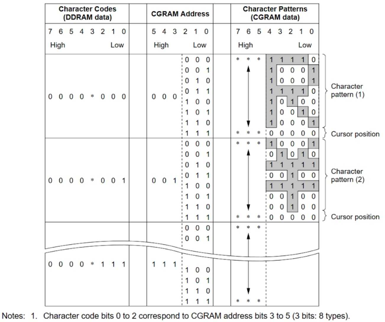
But that’s not all yet. We now need to convert the display_buffer array into another array that is suitable for sending to the CGRAM of the display to generate the characters. In tutorial 19, I already told you how the CGRAM is organized, so you can refer to Figure 4 of it to refresh your memory. As you can see, the characters are generated line-wise, and the display_buffer has the values column-wise. Also, the first element of the CGRAM corresponds to the top line, while the display buffer starts from the bottom. The number of the CGRAM addresses is shown in the last column in Figure 14. In our program, the array character consists of the CGRAM data. This array is two-dimensional. The first group of 8 bytes is used to generate the characters for the first line of the LCD, and the second group of 8 bytes is used to generate the characters for the second line.
The conversion from the display_buffer to the character is not very simple and requires a lot of operations with the bits. Let’s see how it’s done using Figure 14 as an illustration. Let’s start with the bottom row, which corresponds to the seventh byte of the second group of the character array, simply saying - to the character[1][7]. As you can see, this byte can be collected with the bit #0 of the display_buffer[0]-display_buffer[5]:
character[1][7] = (display_buffer[4] & 0x01) + (display_buffer[3] & 0x01) << 1 + (display_buffer[2] & 0x01) << 2 + (display_buffer[1] & 0x01) << 3 + (display_buffer[0] & 0x01) << 4
The bitwise AND operation (&) is used to distinguish the single bit of the array. In our case, it’s bit #0, so we perform the AND operation between the display_buffer element and the number 0x01. After that, we need to shift the distinguished bit to the right place of the character[1][7] byte. As you can see in Figure 5, the display_buffer[0] element corresponds to bit #4 of the character[1][7] byte (compare this image with Figure 4 of tutorial 19).
In the same way, we distinguish the bit #0 in the next display_buffer elements and shift them to the right place. The next character[1] element is calculated similarly:
character[1][6] = ((display_buffer[4] & 0x02) >> 1) + ((display_buffer[3] & 0x02) >> 1) << 1 + ((display_buffer[2] & 0x02) >> 1) << 2 + ((display_buffer[1] & 0x02) >>1) << 3 + ((display_buffer[0] & 0x02) >> 1) << 4
As you see, now we need to distinguish bit #1; that’s why we now use 0x02 in the AND operation. Then we need to put the bits in the right place by the left shift. But as we use the second bit of the display_buffer, we need to shift every bit at one position to the right first. Yeah, I understand. This is complex, so you probably need to think a bit to realize how it’s all done. Believe me; I also spent some time before I managed to do it properly.
Actually, the other character elements are calculated in the same way:
character[1][5] = ((display_buffer[4] & 0x04) >> 2) + ((display_buffer[3] & 0x04) >> 2) << 1 + ((display_buffer[2] & 0x04) >> 2) << 2 + ((display_buffer[1] & 0x04) >> 2) << 3 + ((display_buffer[0] & 0x04) >> 2) << 4...
character[0][1] = ((display_buffer[4] & 0x8000) >> 15) + ((display_buffer[3] & 0x8000) >> 15) << 1 + ((display_buffer[2] & 0x8000) >> 15) << 2 + ((display_buffer[1] & 0x8000) >> 15) << 3 + ((display_buffer[0] & 0x8000) >> 15) << 4
You can notice a pattern here so we can make the conversion in a loop. When we return to the program, I will show you how it’s done. Also, please remember that the display_buffer is not limited to five elements, and we need to generate the characters for the remaining six CGRAM addresses, which I will also show you later.
I have explained everything you need to understand the program code, so let’s return to it. As you remember, we only need to consider the refresh_display function in lines 9-80.
In lines 11-17, we declare the local variables of the function:
- min and max (line 11) are the lower and upper neighboring values in the adc_data array, which I already discussed.
- character array (line 12) is used to generate the characters using the CGRAM of the 1602 LCD. I already explained its use in detail.
- display_buffer (line 13) is a kind of canvas on which we draw the graph. This one is also already explained.
- start_index (line 14) is the number of the element of the adc_data array from which we start its “drawing”. By default, we set it to the middle of the array - 25. It synchronizes the graph view, which I will discuss a bit later.
- max_v (line 15), min_v (line 16), and avg_v (line 17) are the minimum, maximum, and average voltages in the saved chunk of the measurements. We assign the initial value of the adc_data[0] to all of them.
In lines 18-25, there is a loop in which we find the maximum and minimum values and accumulate the average voltage. Please note that we start the loop from 1, not from 0 (line 18), as we have already assigned adc_data[0] to all three variables used. The algorithm is quite straightforward. In line 20, we check if the current element of adc_data is greater than max_v. If so, we assign this element to the max_v (line 21). In line 22, we check if the current element of adc_data is smaller than min_v. If so, we assign this element to the min_v (line 23). In line 24, we added the current adc_data value to the avg_v.
In line 26, we divide the avg_v value by 50 to calculate the average voltage of all 50 elements.
In lines 27-29, we convert the ADC result into a real voltage of 0.1V. As you know, for 10-bit ADC, the voltage is calculated as follows:

In our case, the reference voltage VREF is the difference between the VDD and VSS. As I said, I usually set the PICKit output voltage as 3.25V so that we can consider this value as VREF. Taking this into account, we have:

To get rid of the decimal point, let’s multiply the numerator and denominator by 100:

And as we want to get the voltage is 0.1 V, we need to divide the denominator by 10, so finally, we have:

As you see, this equation perfectly matches the one in lines 27-29.
In lines 30-37, we search for the start element of the array from which we will start drawing the graph. Before considering its implementation, let’s first see what lies under it.
In actual oscilloscopes, you might see the “Trigger” option or “Synchronization.” It is used to steady the image on the oscilloscope screen (I am talking about the periodic input signals). The oscilloscope can start the measurement cycle at any moment during the input signal’s period. So if you display it then as is, it will “jump” after each screen refresh. To avoid this, the oscilloscope reads more samples than can fit into the display and then finds the position in the saved array where the input graph crosses the threshold value in the selected direction (either up or down, this option also is available in real oscilloscopes). Then it outputs the graph from this position.
In real oscilloscopes, the threshold value can be changed. Also, the trigger options are selectable, but for simplicity, they will have a constant threshold level of ¼ of the max input value and the constant synchronization option - “up,” so the graph will be synchronized by its rising edge crossing the threshold.
Let’s now see how it’s done in our program. The logic is the following - we are searching for the synchronization condition in the first 25 elements of the array. If it’s found, we will send the graph from this fount position. If not, we just send the last 25 elements without any synchronization. So, we start the loop to search within the first 25 elements of the array (line 30). In this loop, we check if the current adc_data element is lower than the THRESHOLD and if the next element is greater or equal to the THRESHOLD (line 32). This condition corresponds to crossing the threshold level by the graph from below, and if it meets, we save the current i value as start_index (line 34) and then leave the loop (line 35).
In lines 38-47, there is a loop in which we compose the display_buffer, as I explained earlier. Here we generate 24 elements of the display_buffer (line 38), but the last element will not be displayed, so that it could be omitted. In line 40, we find the minimum value between the current and the next elements of the adc_data:
min = (adc_data[i + start_index] >= adc_data[i + start_index + 1]) ? adc_data[i + start_index + 1] >> 6 : adc_data[i + start_index] >> 6;
Here we use the conditional operation “? :” about which you can read, for instance, here. You see that the adc_data element index is defined here as i + start_index. In this way, we consider the synchronization shift. Also, during the assignment, we shift the adc_data to the right by 6 bits, so the min value will have only 4 higher bits of the result in the range of 0…15.
In line 41, we find the maximum value between the current and the following elements of the adc_data in the same way as the minimum value.
In line 42, we clear the current display_buffer element, as next, we will accumulate the bits in it. In line 43, we start the nested loop from the min value to the max value. Inside this loop, we add to the current display_buffer element the value 1 << j (line 45). This value adds 1 at the bit position defined by the variable j, changing from min to max. By doing this, fill the display_buffer with ones in the bits in places from min to max, the result of which you can see in Figure 5.
Once the display_buffer is filled, we can convert it into a series of characters to send to the CGRAM of the display. We do this in the loop in lines 48-62. As you can see, there are three nested loops.
- The first one (line 48), with the variable k that changes from 0 to 4. This defines the number of characters in a horizontal direction.
- The second loop (line 50) with the variable i that changes from 0 to 8 defines the line number in the current character.
- The final loop (line 54) with the variable j that changes from 0 to 5 defines the number of the bit inside the line in the current character (such as a House that Jack built).
In lines 52-53, we clear the elements of the character array with the indexes [0][7-i] and [1][7-i]. As I already mentioned, the first index defines the number of the 1602 LCD line - 0 for the upper line and 1 for the lower line. The second index defines the number of the line of the character where 0 is the top line and 7 is the bottom line. As discussed and shown in Figure 14, the direction of the bits in the display_buffer and character arrays are the opposite; that’s why we use the index 7-i instead of just i. As i starts from 0, we first will start with the character[x][7] element moving from the bottom to the top.
The most interesting thing happens in lines 56 and 57 of the inner loop. Here, we convert the display_buffer into the character array. Line 56 corresponds to the upper line, and line 57 corresponds to the lower line. The difference between them is that for the upper line we use the index i + 9 (to remind you, this index corresponds to the number of a bit in the display_buffer). If you look at Figure 14, you can see that bit 7 of the character[0] (right column) corresponds to bit 9 of the display_buffer (left column); that’s why we add 9 – other than that, these lines are identical. At first sight, they look monstrous, but they are built based on the formulas I have already provided you for some of the character elements.
Compare these equations
character[1][7] = (display_buffer[4] & 0x01) + (display_buffer[3] & 0x01) << 1 + (display_buffer[2] & 0x01) << 2 + (display_buffer[1] & 0x01) << 3 + (display_buffer[0] & 0x01) << 4
character[1][6] = ((display_buffer[4] & 0x02) >> 1) + ((display_buffer[3] & 0x02) >> 1) << 1 + ((display_buffer[2] & 0x02) >> 1) << 2 + ((display_buffer[1] & 0x02) >>1) << 3 + ((display_buffer[0] & 0x02) >> 1) << 4
character[1][5] = ((display_buffer[4] & 0x04) >> 2) + ((display_buffer[3] & 0x04) >> 2) << 1 + ((display_buffer[2] & 0x04) >> 2) << 2 + ((display_buffer[1] & 0x04) >> 2) << 3 + ((display_buffer[0] & 0x04) >> 2) << 4
with line 57:
character[1][7 - i] += ((display_buffer[4 - j + k * 6] & (1 << i)) >> i) << j;
You can see that they are the same. I just gathered all five components of the sum into a loop. The only difference is the index of the display_buffer: 4 - j + k * 6. The first part (4 - j) should be clear, and it follows from the equations above, and the second part (k * 6) allows us to compose the next characters from the other elements of the display_buffer. As you remember, k changes from 0 to 4, which allows for embracing the display_buffer elements from 0 to 24.
And that’s all about the bits manipulations. After the inner loop, we have the composed character arrays, so now we can invoke the function lcd_create_char to generate the new characters for the upper and lower LCD lines (lines 60-61).
In line 63, we set the cursor at the first position of the first line. Then we send four characters with the addresses 0, 1, 2, and 3 to display (lines 64, 65). These addresses correspond to the characters we have generated for the upper line of the LCD. Then, in line 67, we set the cursor at the first position of the second line and send the next four characters with the addresses 4, 5, 6, and 7 (lines 68, 69), which we have generated for the lower line.
In lines 71-79, we display the min_v, max_v, and avg_v values in the display along with the static text. I don’t see any reasons to consider these lines in more detail, as they are quite clear. If not, please refer to tutorial 23 where the lcd_write_string and lcd_write_number functions are described.
And finally, that’s it! We did it! Surprisingly (in fact - no, not actually that surprising), the description of this program took a lot of time, but you agree - it’s quite complex. Let’s now assemble the circuit according to Figure 1, build and run the program code and make some tests.
Testing of the Oscilloscope
If nothing is connected to the AIN3 pin of the MCU, the result is obvious - we will have 0 everywhere, and the graph will be flat (Figure 15).

For testing the oscilloscope, you now need a signal generator. Fortunately, I have one which is quite simple but works well. It can generate sine, saw, square, and triangle waves with an amplitude of about 3 V - just what we need. If you don’t have any, don’t be upset; in the next tutorial, I’ll show you how to make it based on the same PIC18F14K50 MCU. The other option is to use the sine wave generator we built based on the PIC10F200 MCU.
In Figure 16 I applied the sine wave signal with the 500 Hz frequency to the input AIN3.

Well, figure 16 is the same as Figure 13 but without the red rectangles. The frequency of 500 Hz corresponds to the signal period of 1 / 500 = 0.002s = 2 ms. As you remember, I set the Timer3 period, so each LCD character corresponds to 1 ms. And in Figure 16, you can see that the sine wave has a period of exactly 2 characters which means that the horizontal resolution works properly. As for the vertical resolution, we agreed that each pixel corresponds to 200 mV. In Figure 16, you can see that two upper lines are unused by the graph, so it spends 8 pixels of the bottom character, one pixel between the characters, and 6 pixels of the top character. This gives us 15 pixels, or 15 x 200 = 3000 mV. In the LCD (Figure 16), you can see the maximum measured voltage is 2.9 V which corresponds to the measured one with quite a decent accuracy for such a simple device.
In Figure 17-19, there are saw, triangle, and square signals of the same frequency.


As you can see, all the signals are recognizable even with such a low resolution. Also, you can’t see it in the static figures above, but the signal is relatively steady and doesn’t jump, which means the synchronization works well. You can notice in Figure 16-18, the wave starts at about ¼ of the amplitude, corresponding to the THRESHOLD value set in line 4. You can change it and see how that affects the result.
Figure 20 and 21, show the sine wave signals with 200 Hz and 1 kHz frequencies, respectively.


The signal at 1 kHz looks pretty ugly here, but you still can see that each period here takes exactly one LCD character.
Its value is that the algorithms that lay upon it are used in real oscilloscopes, so you can build an effective working device by using a normal display and adding some controls.
It’s time to finish this tutorial. It would be best if you had some time to understand everything we have done today. As I’ve said from the start, this topic is not easy, but on the bright side (worth bragging), you may use this knowledge to amuse your engineering friends.
As homework, I encourage you to experiment and practice... Fit the whole graph in one LCD line, but prolong it to 8 characters. This will reduce the vertical resolution twice but will expand the whole graph horizontally so that you can see more.

Authored By
Sergey Sokol
I was born, raised, and currently live in Ukraine. I’m fond of different types of electronics and backpacking but these things have been set aside with the war that has been thrust on my country, my people, and my family. Through these trials, if you could help support me financially, I would appreciate any help that could be sent via Paypal to sokolsp@gmail.com

Related Tutorials

Related EE FAQs
 work?")
How do Analog to Digital Converters (ADCs) work?

Answered by Uma Bharathi D

What is the Difference Between Analog and Digital Signal Processing?

Answered by Amrutha Varshini

How should I choose an Oscilloscope?

Answered by Gary Crowell
Explore CircuitBread
- 244 Tutorials
- 9 Textbooks
- 12 Study Guides
- 31 Tools
- 104 EE FAQs
- 295 Equations Library
- 213 Reference Materials
- 97 Glossary of Terms
Friends of CircuitBread
-

Search Hundreds of Component Distributors + 2 Perks
-

Power Supply Related Technical Resources + 1 Perk
-

Free eBook & Resource Library + 1 Perk


Get the latest tools and tutorials, fresh from the toaster.


