The temperature of your room, the sound of sea waves, the intensity of sunlight throughout the day – every environmental observation in the world we live in is in the form of a continuous (in both time and amplitude) analog signal.
Even when we speak over the phone, our speech is analog in nature. Yet we also live in a world of 0s and 1s. This speech (analog signal) is converted into digital bits consisting of 0s and 1s making them suitable to be transferred over a telephone or other digital communication network and the same bits are reconstructed back at the receiver's end and played on a microphone whose output is perceivable audio – an analog signal.
The conversion of an analog signal to a digital one takes place with the help of ADCs or analog-to-digital converters. These are basically sampling and mapping circuits which sample the analog signal at uniform time intervals, and map the obtained sample to digital words made of binary numbers 0 and 1. This gives a digital representation of an analog occurrence.
Having obtained the basic idea behind an ADC, let's now have a look at a simplified schematic of the ADC circuit and discuss each of the blocks in detail.

Sample and Hold Block
Analog signals are continuous in both time and amplitude. The first step in converting an analog signal into a digital signal involves sampling of the analog signal amplitude at regular time intervals.
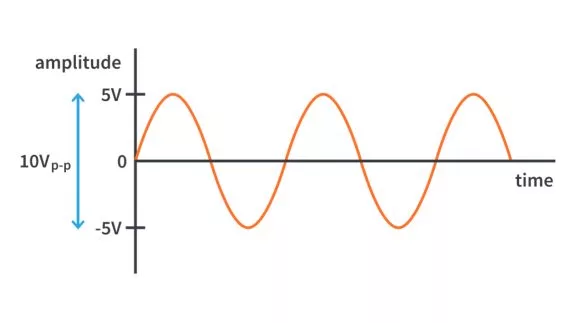
Consider the analog to digital (A to D) conversion of a sine wave. The image given below is of a sine wave, continuous in time and amplitude, taken as our signal.
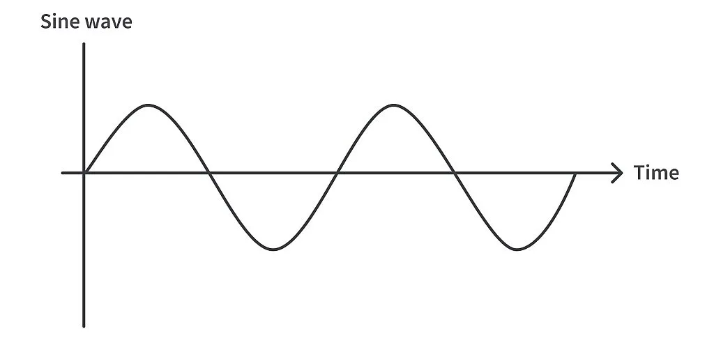
This analog signal is input to the sample block which consists of a sampler switch. The sampler switch is usually a simple switch which closes and opens at the sampling frequency as shown in the image below. When the switch closes, the amplitude of the signal at that point in time is available at the output of the switch. This instantaneous amplitude is fed to the hold block as long as the switch remains closed.
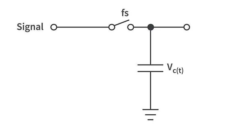
The holding of the sampled value is achieved with the help of a capacitor connected at the output of the sampler switch. As shown in the image above, when the switch closes the capacitor charges to the voltage value of the analog signal at that point in time. The switch can now be opened as the sampling process is complete, the capacitor will stay at the charged value of vc until the next sampling instant – that is, when the switch closes again. The capacitor voltage is now the sampled version of the input signal. The voltage of the capacitor vc i.e., the sampled signal vs time graph is shown below:
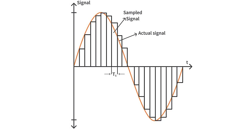
The input sine wave was both continuous in time and amplitude. As the switch closes, the capacitor charges to the voltage at that point, and when the switch opens, it holds on to that voltage until the switch closes again. So, the capacitor voltage is in the form of rectangular strips with height equal to the amplitude of the signal at the start of the sampling interval (when the switch closes). Hence the output voltage (capacitor voltage) is continuous in time and discrete in amplitude. This voltage across the capacitor will be used for further processing.
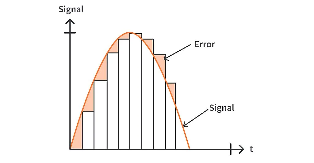
An observation to be made from the animation here is that the samples don’t exactly coincide with the signal amplitude. As shown in the image below, the sampled strips of voltage(black) and the sine wave signal(red) show an evident error(yellow). This error is unavoidable during sampling and can be minimised by increasing the sampling frequency. But increasing the sampling frequency too much will just lead to increased processing and more storage.
Quantize Block
The input to the quantize block is the output voltage of the capacitor. The output voltage of the capacitor is in the form of rectangular strips across time whose amplitude remains constant throughout each sampling interval. Each strip (corresponding to each sampling interval) is now mapped to an equivalent binary number value comprising of 0s and 1s.
Let’s understand the quantization process with the help of an example.
For this example, let’s consider a 3-bit ADC with an input voltage ranging from 0V to 1V. These specifications mean that the input voltage should range between 0V at the minimum to 1V at the maximum. The full voltage range of 0V to 1V will be mapped to a 3-bit binary number from 000 to 111 (each of the 3 places can either be a 0 or a 1: 2x2x2 = 8 binary numbers).
The resolution of the ADC for these parameters is

The resolution gives the minimum amount of voltage which is required to change the output of the ADC. Say the signal amplitude is about 0V, then the digital mapped number will be 000. Since our resolution is 0.125V, for all values of input signal amplitude between 0V to 0.125V, the output digital number will be 000. For a voltage above 0.125V to 0.250V, the mapped value will be 001. For signal amplitude between 0.250V to 0.375V, the output digital number will be 010. The transfer curve for the above conversion will be as shown in the image below:
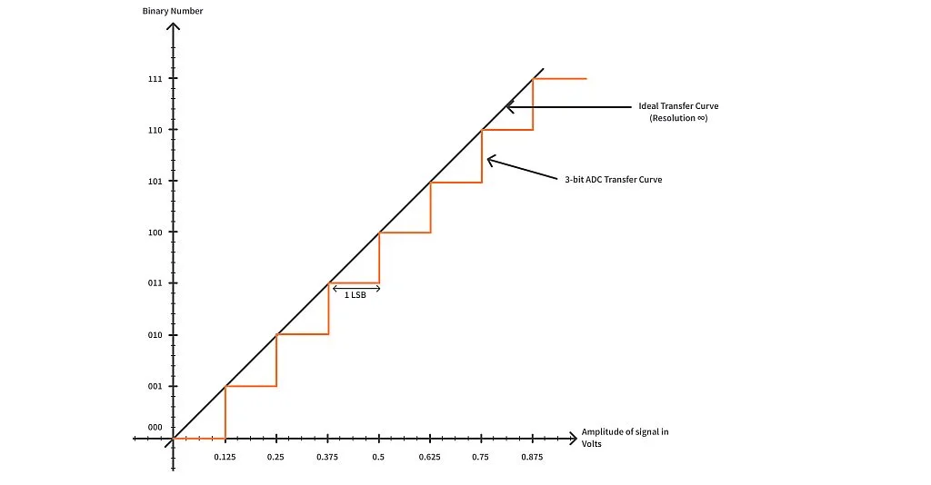
It is here that we talk about quantization error. For an amplitude of the analog signal of value anywhere between 0V to 0.125V, the output is the same – 000. This leads to loss of information as any value between 0V to 0.125V is treated the same. In terms of voltage, the quantization error is 0.125V.
The quantization error can be reduced by decreasing the resolution voltage i.e., adding more bits in the digital output for the same input voltage.
The output from the quantization block is values of digital words, these are then cascaded and converted into a stream of bits for transfer through serial networks. The bits are obtained and then the signal can be reconstructed at the receiving side.
The resultant digital binary numbers can be output either in series or parallel. Parallel output requires a separate pin for each of the binary digits ultimately increasing the size of the ADC chips. Serial output requires just one pin and is more economical to manufacture.
The application of ADC is wide ranging. A basic and common example is in a microcontroller - we interface sensors which record analog data. ADCs come mounted on the microcontrollers converting the recorded analog data to digital bits for further processing. Air conditioners, cameras, oscilloscopes – almost all devices and gadgets available in the market employ some digital operation and use ADCs in them. Understanding how they work and their limitations can be incredibly useful in beneficial utilization of these modules in designs.
