Generating Waveforms with the DAC module Using MCC | Embedded C Programming - Part 31
Published
Hello again! This tutorial is the final one devoted to the analog modules of the PIC18F14K50 MCU. In it, we will consider the voltage reference modules. I have already mentioned them in the previous two tutorials, and now the time has come to familiarize you with them in more detail.
So PIC18F14K50 has two voltage references: a fixed voltage reference of 1.024 V and a programmable voltage reference whose voltage can be changed within 32 steps. So the latter is often called the 5-bit digital-to-analog converter (DAC).
In this tutorial, we will use them both to build the signal generator to produce sine, saw, or triangle waveforms with different frequencies. The type of the signal and the frequency will be displayed in the same 1602 LCD we used before. Changing the frequency and waveform will be implemented by means of two buttons.
Traditionally, let’s first get familiar with the new modules used in the current project. Their description won’t take long as they are quite simple.
Fixed Voltage Reference (FVR) Module
Actually, both voltage references are considered as two parts of the same module but let’s split their description not to mix up what is what.
FVR (as follows from its name) is the stable, fixed, VDD-independent reference voltage source. Its nominal voltage is 1.024 V but can be multiplied by 2 or 4. In the last case, the VDD voltage should be higher than the desired reference voltage.
The FVR voltage can be used as the reference voltage for the analog comparator, ADC, or DAC modules.
After the FVR module is enabled, it takes some time before the output voltage is stabilized, so it would be good to provide some small delay waiting while it becomes stable.
Programmable Voltage Reference, or Digital-to-Analog Converter (DAC) Module
This module operates independently from other analog modules, meaning it can be turned on or off separately at any moment. As I mentioned before, it provides 32 voltage levels, which the following equation can calculate:

where


DAC1R is the value of the DAC1R register, which can have values from 0 to 31 and sets the output voltage of the DAC module.
The positive and negative reference voltages are selectable, like in the ADC module.
The output voltage of the DAC module can be driven to the positive input of the analog comparator. Also, the output voltage can be output to the pin CVREF which is merged with the RC2. The DAC’s current drive ability is quite low, so you can’t connect it to the low-resistance load. To do this, you need to use some external buffer like the operational amplifier connected as the voltage follower (Figure 1, copied from Figure 21-2 of the PIC18F14K50 data sheet).

The capacitor at the output of the DAC module, along with the internal resistance R, works as a low-pass filter smoothing the steps of the DAC voltage levels. We proved its effectiveness when we created the sine wave generator based on the PIC10F200 MCU.
And that’s enough information about the voltage reference modules to write the program that uses them. As usual, please refer to Chapter 21 of the PIC18F14K50 data sheet for more information.
Schematic Diagram
The schematic diagram is shown in Figure 2.
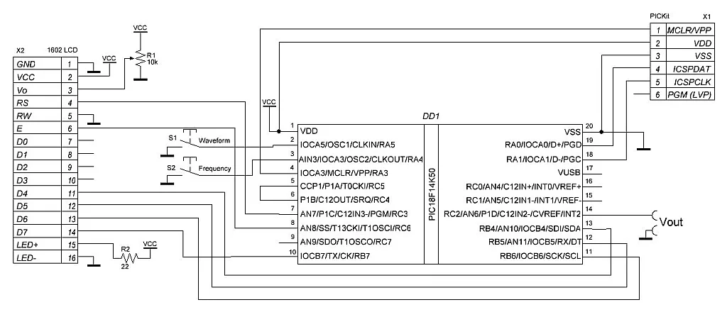
This schematic diagram is very similar to the one presented in tutorial 24, but it has some extra parts: it consists of the PIC18F14K50 MCU (DD1) and 1602 character LCD (X2), which are connected in the same way as there. Also, it has two push buttons - S1 for setting the waveform and S2 for setting the frequency. The DAC output is read by the oscilloscope from the pin RC2/CVREF. In this schematic, the filtering capacitor is absent to see the raw output waveform; also, the output buffer (like in Figure 1) is absent because the oscilloscope input has very high resistance. You should add these parts to an actual signal generator for proper operation.
That’s everything about the device schematic diagram so we can proceed to the next step.
Configuration of the Project using MCC
Let’s create a new project now. I’ve called it “Signal_generator_MCC” but you can give it any name you want.
We must configure Timer2, DAC, and FVR modules with the MCC in this project. The timer will be needed to send the next value into the DAC in the specified time intervals, so the generated signal will have a stable frequency.
Let’s create a new project, run the MCC plugin, and change the MCU package. Open the System Module page, set the Internal Clock as 8MHz_HF, and set the “PLL Enabled” checkbox . Also (as usual), don’t forget to remove the check from the “Low-voltage programming enable” field (Figure 3).

Then we need to go to the Device resources tab on the left part of the screen, expand the drop-down list “Timer," and click on the green plus at “TMR2” (Figure 4).

There was actually a weird thing with the timers. I intended to use any but Timer2 initially because all of them except Timer2 can work in 16-bit mode, so we can achieve the required time step without changing the timer’s prescaler. But for some reason, when I used these timers, I couldn't achieve the desired frequency, as it was always smaller. And this problem persisted with Timer0, Timer1, and Timer3. I was ready to believe that this was the issue of the internal oscillator accuracy, but then out of desperation, I decided to try Timer2, and suddenly it turned out that with it, the frequency fits ideally, which surprised me a lot. The configuration of this timer is more complex than others because it has a resolution of just 8 bits, so we need to change the prescaler and postscaler for every frequency. But as it was the only working solution, I had to deal with it. Well, that was a lyrical digression, and now let’s return to the configuration.
Next, we need to expand the “FVR” list and add the “FVR” position (Figure 5).

Finally, we need to expand the “DAC” list and add the “DAC (5 bit)” position (Figure 6).

After that, your Resource Management window should look like in Figure 7.

Now, let’s open the TMR2 window and configure the Timer2 module according to Figure 8.

We considered this timer in detail in the tutorial 23.
Here Timer2 will be used as a timer that generates the interrupts in a defined interval. When these interrupts happen, we will update the DAC value. So using the timer, we can be sure that the generation of the signal will be done with a constant period.
As for the timer period value, I will explain it later, when we consider the program code. Moreover, it will be variable because we want to generate the signals with the different frequencies. And even moreover, we will need to manually change the prescaler and postscaler values using the direct registers manipulation because MCC doesn’t provide the required functions to do this.
Now, let’s switch to the FVR tab and configure the FVR module (Figure 9).

As you can see, the FVR module has very few options:
- “Enable FVR” - enables the FVR module.
- “FVR buffers to ADC, DAC, and CMP” - sets the output voltage of the FVR module which can be 1.024 V (1x), 2.048 V (2x), or 4.096 V (4x). In our case we select 2.048 V because 1.024 V is too few, and 4.096 V can be too much especially when using the supply voltage as 3.3 V like I do.
The last module to configure is DAC (Figure 10).

The DAC module has more options but they all are quite simple:
1. “Enable DAC” enables the DAC module.
2. “Positive Reference” sets the positive reference source for the DAC module. The available options are: internal reference from VDD (“VDD”), internal reference from the FVR output (“FVR_buf1”) and external reference from the VREF+ pin (“VREF+”). We will select the second option (“FRV_buf1”) to have the stable amplitude of the output signal even if the MCU supply voltage deviates.
3. “Negative Reference” sets the negative reference source for the DAC module. The available options are: internal reference from VSS (“VSS”), and external reference from the VREF- pin (“VREF-”). Here we leave the “VSS” option as we’re not going to apply any external reference voltage.
4. “Low-Power Voltage State” selects the output state of the DAC when the MCU is in the low-power mode. There are two available options: “neg_ref” which sets the DAC output equal to the negative voltage reference (in our case it would be VSS), or “pos_ref” which sets the DAC output equal to the positive voltage reference (in our case it would be FRV output, which I’m not sure if it stays active in the low-power mode). As our device is not going to operate in the low-power mode, we can leave this option unchanged.
5. “Enable Output on DACOUT”. If this checkbox is set then the DAC output is connected to the RC2/CVREF pin. In this case, the digital buffer of this pin is disabled, and the reading of its input register will always be 0. If the checkbox is clear, the RC2/CVREF pin is disconnected from the DAC output and can be used as a regular GPIO pin. We’re going to forward the DAC output outside the MCU, so we need to set this checkbox.
For some reason in my current version of the MCC this checkbox has no effect, so in order to enable the DAC output pin we need to switch to the “Register” tab and select the “Enabled” at the “DAC1OE” field (Figure 11).

6. “Software settings” block is an optional one. It allows you to estimate if you can achieve the required output voltage using the given settings of the reference voltages and set the initial state of the DAC output. We’re not going to use this feature, so we leave this block unchanged.
Now, let’s switch to the Pin Module and Pin Manager and configure all required pins according to the schematic diagram (Figure 12).

Here we can see the familiar LCD pins D4, D5, D6, D7, RS, and E which are connected the same as in several previous tutorials, to the pins RB4, RB5, RB6, RB7, RC3, and RC6 of the MCU, respectively.
The RC2 pin is now controlled by the DAC module and has the “DACOUT” function. We don’t need to do anything with it here, as its configuration has been done earlier when we enabled the DACOUT pin in the DAC module configuration (Figure 11).
Also there are two input pins RA4 (BUT_FREQ) and RA5 (BUT_FORM) to which the buttons S2 and S1 are connected, respectively (see Figure 2).
Don’t forget to enable the pull-up resistors on these pins, and also to enable the pull-up resistors for ports A and B (bit nRABPU of the INTCON2 register) (Figure 13). If you forget about that, the MCC will show the corresponding warning.

Finally, let’s switch to the Interrupt Module tab and make sure that the Timer2 interrupt is enabled (Figure 14).

There is no need to enable the priorities of the interrupts as only one of them is active.
Now everything is configured, and we can click the “Generate” button and switch to code writing.
Program Code Description
The same as in tutorials 23 and 25, we will need to copy and paste the “lcd_1602_mcc.h” and “lcd_1602_mcc.c”. One can take them from tutorial 23 or 25, as I showed you. After all, your project should look like in Figure 15

If you compare the schematic diagrams (Figure 2) in the current tutorial and Tutorial 25, you will notice that the connection of the display is equal, so if you took the LCD-related files from them, you don’t need to make any changes to them. And if you copied them from one of the previous tutorials, please remember to change the pin assignment; otherwise, your display won’t work properly.
Now let’s consider the “main.c” file and write the following code.
#include "mcc_generated_files/mcc.h"
#include "lcd_1602_mcc.h"

uint8_t waves_5b[3][32] = {{16, 19, 21, 24, 26, 28, 30, 31, 31, 31, 30, 28, 26, 24, 21, 19,
                        16, 12, 10,  7,  5,  3,  1,  0,  0,  0,  1,  3,  5,  7, 10, 12}, //Sine
                       	{ 0,  2,  4,  6,  8, 10, 12, 14, 16, 17, 19, 21, 23, 25, 27, 29,
                        31, 29, 27, 25, 23, 21, 19, 17, 16, 14, 12, 10,  8,  6,  4,  2}, //Saw
                       	{ 0,  1,  2,  3,  4,  5,  6,  7,  8,  9, 10, 11, 12, 13, 14, 15,
                        16, 17, 18, 19, 20, 21, 22, 23, 24, 25, 26, 27, 28, 29, 30, 31}};//Triangle

uint16_t frequencies[6] = {2000, 1000, 500, 200, 100, 50};  //Supported frequencies in Hz
uint8_t pr2[6] = {124, 249, 249, 249, 249, 249};//Value of the Timer2 period
uint8_t postscaler[6] = {0, 0, 1, 4, 9, 4};             //Value of the Timer2 postscaler
uint8_t prescaler[6] = {0, 0, 0, 0, 0, 1};              //Value of the Timer2 prescaler

volatile uint8_t wave_index;  //Index of the waveform in the waves_5b array
uint8_t index;                          //Index of the element within one waveform
uint16_t frequency_index;      //Index of the element of the frequencies array

void timer2_isr_handler (void)
{
    DAC_SetOutput(waves_5b[wave_index][index]);         	//Copy the current element of the waves_5b array to the DAC
    index ++;                                           	//Increment the index to set the next element of the waves_5b array the next time
    if (index == 32)                                 //If index is 32 (the limit of the array)
        index = 0;                                      	//Then set index as 0
}

void refresh_lcd (void)                                 	//Refresh the LCD information
{
    lcd_clear();                                        	//Clear the LCD
    lcd_write_string("Waveform:");                      	//Write the "Waveform" text
    switch (wave_index)                                 	//If wave_index is...
    {
        case 0: lcd_write_string("SINE"); break;        	//0 then write "SINE"
        case 1: lcd_write_string("TRIANGLE"); break; //1 then write "TRIANGLE"
        case 2: lcd_write_string("SAW"); break;         //2 then write "SAW"
    }
    lcd_set_cursor(1, 2);         	//Set cursor at the beginning of of the next line
    lcd_write_string("Frequency:");                     	//Write the "Frequency" text
    lcd_write_number(frequencies[frequency_index], 0);  	//Write the value of the frequency from the array
    lcd_write_string("Hz");                             	//Write the "Hz" text
}

void main(void)
{
    SYSTEM_Initialize();                                	//Initialize the system
    TMR2_SetInterruptHandler (timer2_isr_handler); //Set the Timer2 interrupt handler
    lcd_init(0, 0);             //Initialize the LCD without cursor and blinking

    INTERRUPT_GlobalInterruptEnable();   //Enable global interrupts
    INTERRUPT_PeripheralInterruptEnable();   //Enable peripheral interrupts

    frequency_index = 0;            //Set the frequency_index as 0
    wave_index = 0;                     //Set the wave_index as 0

    refresh_lcd();                         	//Write the initial text at the LCD

    while (1)
    {
        if (BUT_FORM_GetValue() == 0)     	//If the waveform button is pressed
        {
            __delay_ms(20);                             	//Then perform the debounce delay
   	if (BUT_FORM_GetValue() == 0)    //If after the delay button is still pressed
   	{
       	    while (BUT_FORM_GetValue() == 0);  //Then wait while button is pressed
       	    __delay_ms(20);  //After button has been released, perform another delay
       	    if (BUT_FORM_GetValue() == 1)    //If the button is released after the delay
       	    {
           	        wave_index ++;            //Increment the wave_index
                    if (wave_index == 3)      //If wave_index is 3 (the last element in the waves_5b array)
                    wave_index = 0;       //then set the wave_index as 0
                    refresh_lcd();            //Update the LCD information
       	    }
            }
        }

        if (BUT_FREQ_GetValue() == 0)  	//If the Frequency button is pressed
        {
            __delay_ms(20);                             	//Then perform the debounce delay
           if (BUT_FREQ_GetValue() == 0)    //If after the delay button is still pressed
           {
       	    while (BUT_FREQ_GetValue() == 0);    //Then wait while button is pressed
       	    __delay_ms(20);    //After button has been released, perform another delay
       	    if (BUT_FREQ_GetValue() == 1)  //If the button is released after the delay
       	    {
           	        frequency_index ++;   //Increment the frequency_index
                    if (frequency_index == 6)   //If frequency_index is 6 (the last element in the frequencies array)
                    frequency_index = 0;            	//then set the frequency_index as 0
                   TMR2_LoadPeriodRegister(pr2[frequency_index]); //Copy the corresponding element of the pr2 array into the Timer2 period register
                    T2CONbits.T2OUTPS = postscaler[frequency_index]; //Copy the corresponding element of the postscaler array into the T2OUTPS bits of the T2CON register
                    T2CONbits.T2CKPS = prescaler[frequency_index];  //Copy the corresponding element of the prescaler array into the T2CKPS bits of the T2CON register
                    refresh_lcd();                      	//Update the LCD information 	    }
            }
        }
    }
}
In line 1, we, as usual, include the “mcc_generated_files/mcc.h” file to be able to use the MCC-generated variables, functions, and macros. In line 3, we include the “lcd_1602_mcc.h” file, which consists of the 1602 LCD-related functions.
In line 4, we declare the waves_5b array of the uint8_t type. This array is two-dimensional. It consists of 3 one-dimensional arrays, each of which consists of 32 values. Elements of the waves_5b array represent the values of the DAC1R register, which allow to generate the desired waveform.
Let’s briefly consider how it works. Generation of any waveform represents the continuous calculation of the signal amplitude with the fixed time step and converting this amplitude into the DAC voltage using the equation (1). For sure, we can calculate the amplitudes on the fly, but this can significantly reduce the maximum frequency because the mathematical calculations take a lot of time (especially for a sine wave). So in practice, the period of the function is divided into some parts. The more parts provided, the better the waveform quality, but this also decreases the maximum frequency. In our case, I divided the whole period into 32 parts and calculated the DAC1R values for each of the three supported waveforms.
Let me show an example of the generation of the sine waveform. As you know, the sin(x) function has the ranges [-1; 1], so -1 of the sin(x) should correspond to 0 of DAC1R, and 1 of sin(x) should correspond to 31 of DAC1R. Here we can use the formula of linear interpolation:

As we know, the sinusoidal period is 

The same with other waveforms. I won’t reproduce all the calculations here. You can treat it as an exercise in mathematical calculations by yourself if you want. As it is, you can see all the data points within the program code itself: the sine wave values are located in waves_5b[0] (lines 4-5), the saw wave values are located in waves_5b[1] (lines 6-7), and the triangle wave values are located in waves_5b[2] (lines 8-9).
In lines 11-18, the global variables are located:
- The frequencies array (line 11) consists of six elements that represent the frequencies that the device can generate. This array is needed only to display the current frequency in the LCD.
- The pr2 (line 12), postscaler (line 13), and prescaler (line 14) arrays also consist of six elements and are used to configure Timer2, which is used to provide stable time steps to generate the waveforms. Each set of elements sets the frequency corresponding to the element in the frequencies array. For example, to generate the frequency of 2000 Hz, you need to set the timer period register PR2 value as 124, the postscaler value as 0, and the prescaler value as 0. We will talk about these values in more detail later.
- The wave_index variable (line 16) is used as the number of the part of the waves_5b array from which the data is currently taken and, thus, corresponds to the type of waveform. You can see that this variable has the volatile modifier, which is needed because it will be used both in the main program and the interrupt subroutine, and without this modifier, the compiler would consider it as two different variables.
- The index variable (line 17) is the number of the element of the subarray of the waves_5b array, which is currently copied into the DAC1R register.
- The frequency_inxed (line 18) is the number of the element in the arrays frequencies, pr2, postscaler, and prescaler. This variable is used to set and display the proper frequency.
In lines 20-26, there is the Timer2 interrupt handler timer2_isr_handler which we will consider later. In lines 28-42, there is the function refresh_lcd which we will also consider later.
And now, let’s switch to the main function of the program (lines 44-97), and particularly to its initialization part (lines 46-56).
In line 46, there is the MCC-generated function SYSTEM_Initialize which initializes all the hardware modules of the MCU.
In line 47, we define the function which will play the role of the Timer2 overflow interrupt handler. As you see, this will be the function timer2_isr_handler which I have already mentioned, and which is located at lines 20-26.
I think now we got to the part where I owe you the explanation of how the values of the arrays pr2, prescaler, and postscaler have been calculated on the example of their first elements, which are 124, 0, and 0, respectively. These values correspond to the signal frequency of 2000 Hz (the first element of the array frequencies). Each signal period is divided into 32 parts (because we use 32 values in the array waves_5b to generate the waveforms). So to generate the signal with the frequency of 2000 Hz, we need to load the new values into the DAC1R register with the frequency of 2000 x 32 = 64000 Hz. This frequency corresponds to 1 / 64000 Hz = 15.625 us (which we set during Timer2 configuration, Figure 8). The clocking frequency of Timer2 is Fosc / 4 = 32 MHz / 4 = 8 MHz, so each timer tick takes 1 / 8 = 0.125 us. And thus, to provide the period of 15.625 us, we need 15.625 / 0.125 = 125 ticks. As the timer reloads when it counts down to 0, we need to start counting from 125 - 1 = 124, which we load into the PR2 register.
Let’s also see how the lowest frequency of 50 Hz can be achieved. Now the desired timer period is 1 / (50 x 32) = 625 us, and the number of ticks of the timer should be 625 / 0.125 = 5000, which definitely can’t be achieved by an 8-bit timer. Both prescaler and postscaler can divide the frequency maximum by 16. To maintain the accuracy, we should use the minimum required dividers. If we use the postscaler of 1:16, then the timer’s period will be 16 times longer, and thus the number of required timer ticks will be 5000 / 16 = 312.5. First, this value is not an integer which doesn’t suit us; second, it still doesn’t fit into the 8-bit value. Let’s then use the first prescaler value of 1:4. In this case, the input timer frequency will be 8 / 4 = 2 MHz, and the timer tick will take 1 / 2 = 0.5 us. In this case, we will need 625 / 0.5 = 1250 ticks. If we divide this number by 256, we can get the minimum required postscaler value: 1250 / 256 = 4.89, which we round to the nearest greater integer value, which is 5. Thus, the number of timer ticks, in this case, will be 1250 / 5 = 250, which now perfectly fits into 8-bit. And now, we need to convert these numbers into the register values. The PR2 value should be 250 - 1 = 254. The T2CKPS value corresponding to the 1:4 divider is 1, and the T2OUTPS value that corresponds to the 1:5 divider is 4. You can see these values as the last elements of the corresponding arrays. The other values are calculated similarly. As we made things clear, let’s return to the program.
In line 48, we initialize the 1602 LCD without the cursor and blinking.
In line 50, we enable all unmasked interrupts, and in line 51, we enable the peripheral interrupts.
In lines 53 and 54, we assign 0 to the variables frequency_index and wave_index, respectively, to start with the sine wave with the 2000 Hz frequency.
In line 56, we call the function refresh_lcd to write the information about the waveform and the frequency at the LCD.
That’s all about the initialization. The main loop of the program is located in lines 58-96.
Everything we do inside the main loop is checking if any button is pressed and processing it. The S1 button (Waveform) is processed in lines 60-75. Here is the standard blocking algorithm, which we considered a lot of times, so I will only stop the action performed when it’s pressed (lines 69-72).
In line 69, we increment the wave_index variable to switch to the next waves_5b subarray and thus to generate the next waveform. If the value of the wave_index becomes 3 (line 70), which means that we run out of the array boundaries, then we set it as 0 (line 71) to return to the first subarray. Then, after all the manipulations, we update the LCD information (line 72).
The payload of the S2 button (Frequency) processing (lines 77-95) is located in lines 86-92 and is similar to the previous one. We first increment the frequency_index (line 86), then we check if it becomes 6 (line 87), and if yes, we set it as 0 (line 88). Now, we need to update the Timer2 period registers PR2. We can do this using the MCC generated function TMR2_LoadPeriodRegister (line 89). It has only one argument - the period value which apparently should be a single-byte value, as the Timer2 is an 8-bit one.
Unfortunately, MCC doesn’t generate similar functions to set the prescaler and postscaler of Timer2, so we need to change them by manipulating directly with the registers. Both these parameters are located in the same register called T2CON. The bits responsible for the postscaler are called T2OUTP2, and we set them in line 90. The bits responsible for the prescaler are called T2CKPS and are set in line 91. After these changes, our device will generate the signal with the new frequency.
Finally, we update the LCD information by calling the refresh_lcd function (line 92).
That’s everything about the main function of the program. Let’s now consider the Timer2 Interrupt handler (lines 20-26).
First, we copy the current element of the waves_5b array into the DAC1R using the MCC generated function DAC_SetOutput (line 22) after which the DAC updates its output voltage. Then we increment the index variable (line 23), check if it becomes 32 (line 24), and if yes, then we assign 0 to it (line 25).
Finally, let’s consider the refresh_lcd function (lines 28-42). In the previous tutorial, the eponymous function was very complex and tangled. Here it’s extremely straightforward. I don’t know if it requires any clarification, so let’s do it briefly. First, we clear the LCD and set the cursor at the first position of the first line (line 30). Then we write the static text “Waveform:” (line 31) and add the waveform type according to the wave_index variable value (lines 32-47). Then we move the cursor to the first position of the second line (line 38), write the static text “Frequency:” (line 39), and add the frequency value from the frequencies array, which corresponds to the frequency_index value (line 40). Finally, we add the static text “Hz” (line 41).
That’s everything about the program code. As you can see, it’s quite simple but requires some preparations, like calculating the DAC values for different waveforms and the timer parameters for different frequencies. Let’s now proceed to the testing of our device.
Testing of the Signal Generator
Let’s now assemble the device according to Figure 2, compile and build the project and flash it into the PIC18F14K50 MCU. If everything is assembled and programmed correctly, you should see the following text on your LCD (Figure 16).

When you press the buttons, the text should be changed: the waveform should change in the following loop: SINE-TRIANGLE-SAW, and the frequency in the following one: 2000Hz-1000Hz-500Hz-200Hz-100Hz-50Hz. For example, this is how the screen looks after several presses (Figure 17).

But for proper device testing, you need to connect the oscilloscope to the RC2/CVREF pin of the MCU to see the real waveforms generated by it. If you don’t have one, you can use the primitive oscilloscope that we have assembled in the previous tutorial, but you will not see the details of the signal in it.
I’ve owned the DS203 oscilloscope for many years. Now it has become obsolete, and I’m pretty sure you can’t buy it, but even something primitive from AliExpress or Amazon (for example, DSO138 (Figure 18), which costs less than $20) will work out for this case.

So, I wanted to complain about my DS203. For some reason, it doesn’t make screenshots anymore. Well, it makes them, but they can’t be read from the internal memory, which is unfortunate, so the next images are just photos of the oscilloscope screen, not the real screenshots, which I liked more. But we have what we have.
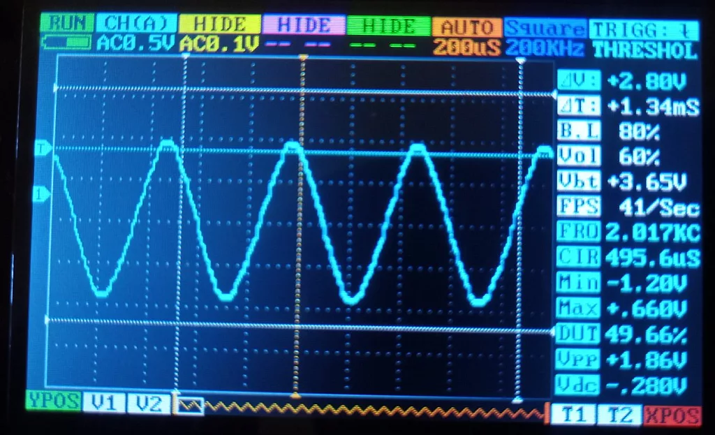
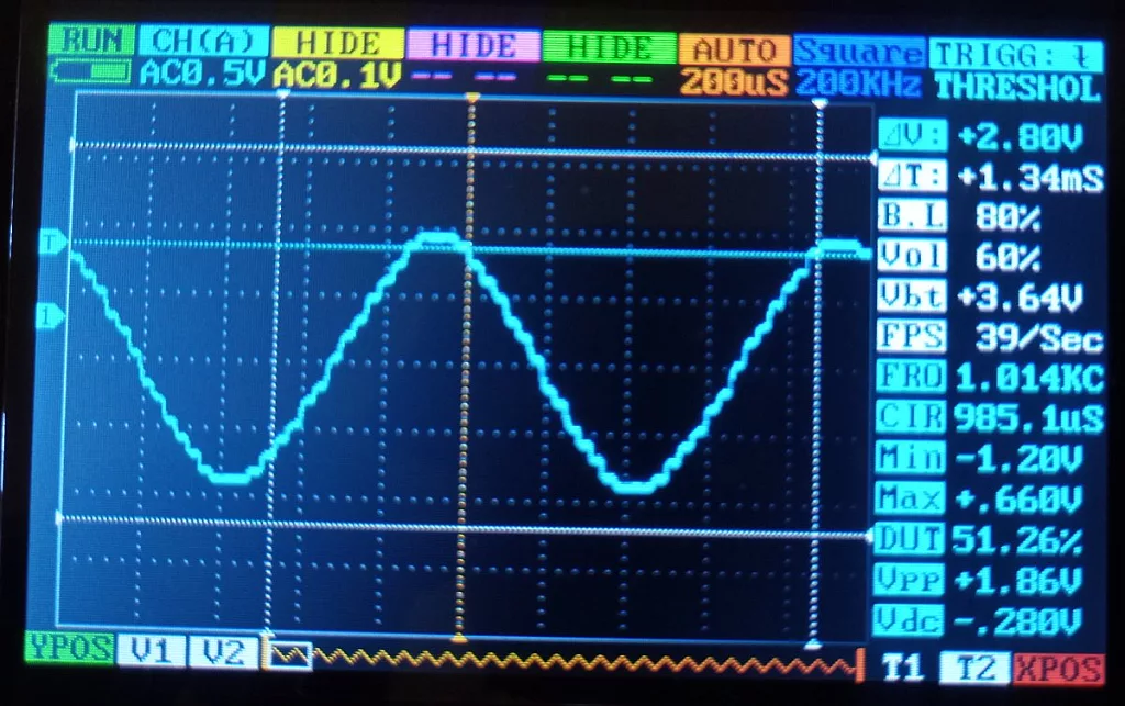
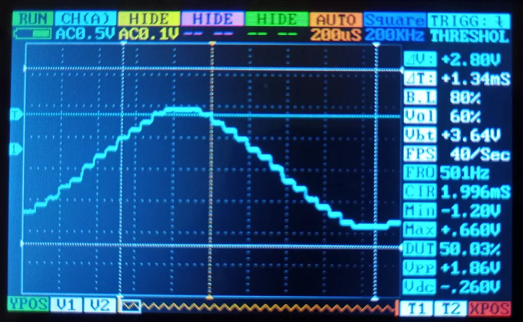
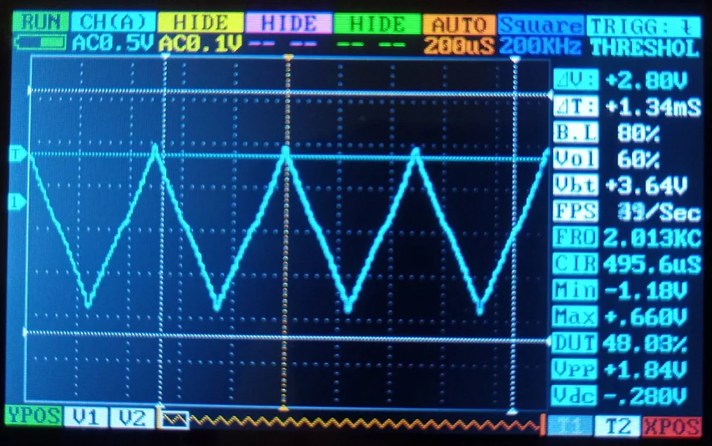
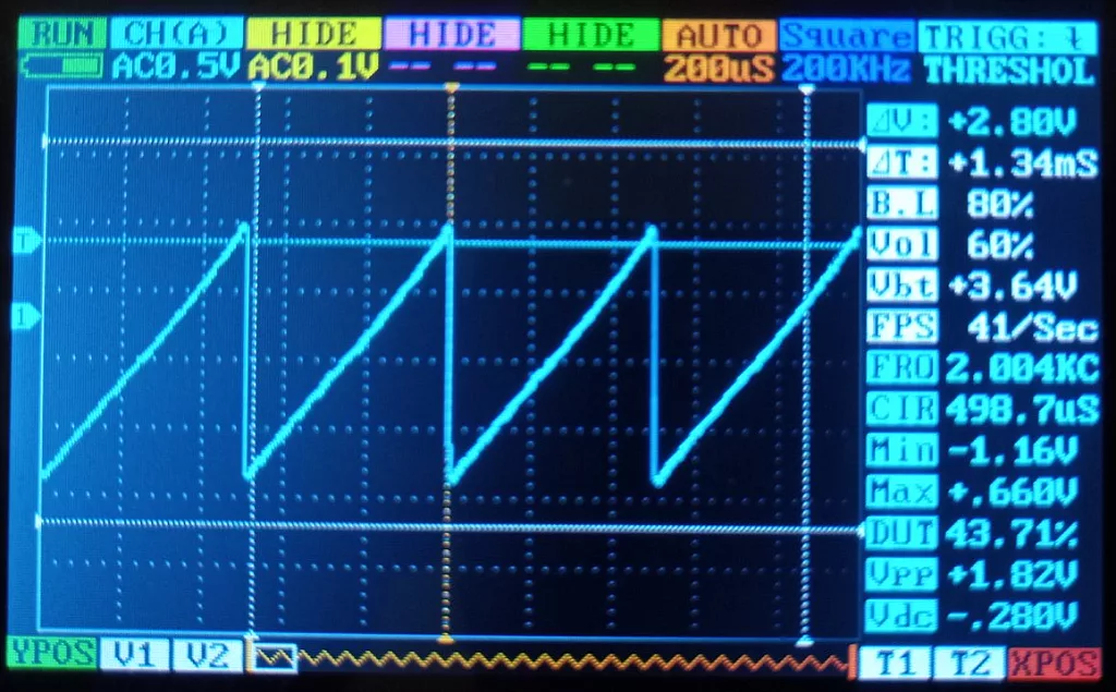
So the following are several photos of the oscilloscope screen for different waveforms and frequencies (Figure 19-23).
What can be concluded from these images?
- The signal forms are close to the desired but are still stepped, which is especially noticeable in Figure 21. Actually, the other signals are the same stepped, but it’s not that noticeable with this horizontal resolution. As I said, to reduce these steps, we need to connect the filtering capacitor between the output of the DAC and the ground. The value of this capacitor is discovered empirically and should be a manageable size - several tens or hundreds of pF, most likely.
- The frequency of the signals is very close to the desired one. You can see it in the right part of the screen as the parameter “FRQ”. For a 2 kHz signal measured frequency varies from 2.004 to 2.017 kHz, which gives the max relative error of 0.017 / 2 x 100% = 0.85%. With the other timers, this error reached several percent.
- The signal’s amplitude is also close to the calculated one which is 1.984 V but is always smaller. You can see its value in the right part of the screen as the parameter “Vpp”. In Figure 7-11, it varies from 1.82 to 1.86 V, which gives the maximum relative error of (1.984 - 1.82) / 1.984 x 100% = 8.3 %, which is quite high. I don’t know what causes such a deviation - the FVR error measurement and calculation error, or even both.
And that’s finally it. In this tutorial, we have familiarized ourselves with the voltage reference modules of the PIC18F14K50 MCU. The programmable voltage reference can be used as a low-resolution 5-bit DAC, which still can produce quite decent waveforms, especially along with the external capacitive filter and the output buffer.
As homework, I suggest you add more waveforms, like a trapezoid or backward saw or whatever you want, and also make more signal frequencies.

Get the latest tools and tutorials, fresh from the toaster.


