Today, let’s learn about the IGBT - the Insulated Gate Bipolar Transistor. The IGBT is a power semiconductor device used in high voltage and high current applications. They’re mainly used as switches in power electronic circuits. Did you notice that in the name of IGBT, there’s an insulated gate like in a FET and a bipolar transistor like in BJT? This is not a coincidence, and the IGBT is indeed a device fabricated trying to include the best of both transistors - particularly the MOSFET and the BJTs - making it worth looking at them from a semiconductor perspective.
Before we begin exploring the details of the IGBT, it might be beneficial to review the basics of semiconductors. We have a collection of several detailed tutorials dealing with semiconductor physics from the most basic principles.
Basics of IGBT
Look at the image below. Since the IGBT is a mix of the FET and the BJT, the symbol also represents this combination. A p-channel IGBT can also be represented similarly.
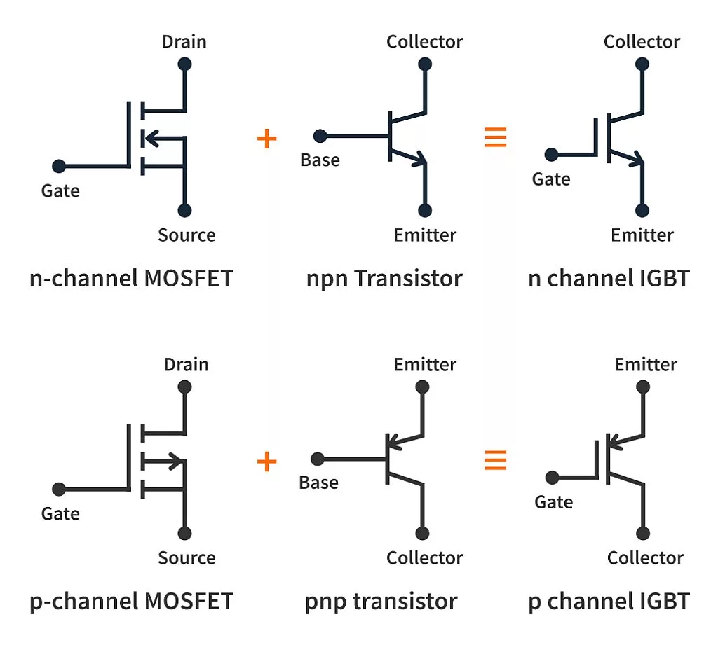
The IGBT has collector and emitter terminals similar to the BJT, where the actual current flows and an insulated gate instead of a base for controlling the device on and off.
Fabrication of the IGBT and its Structure
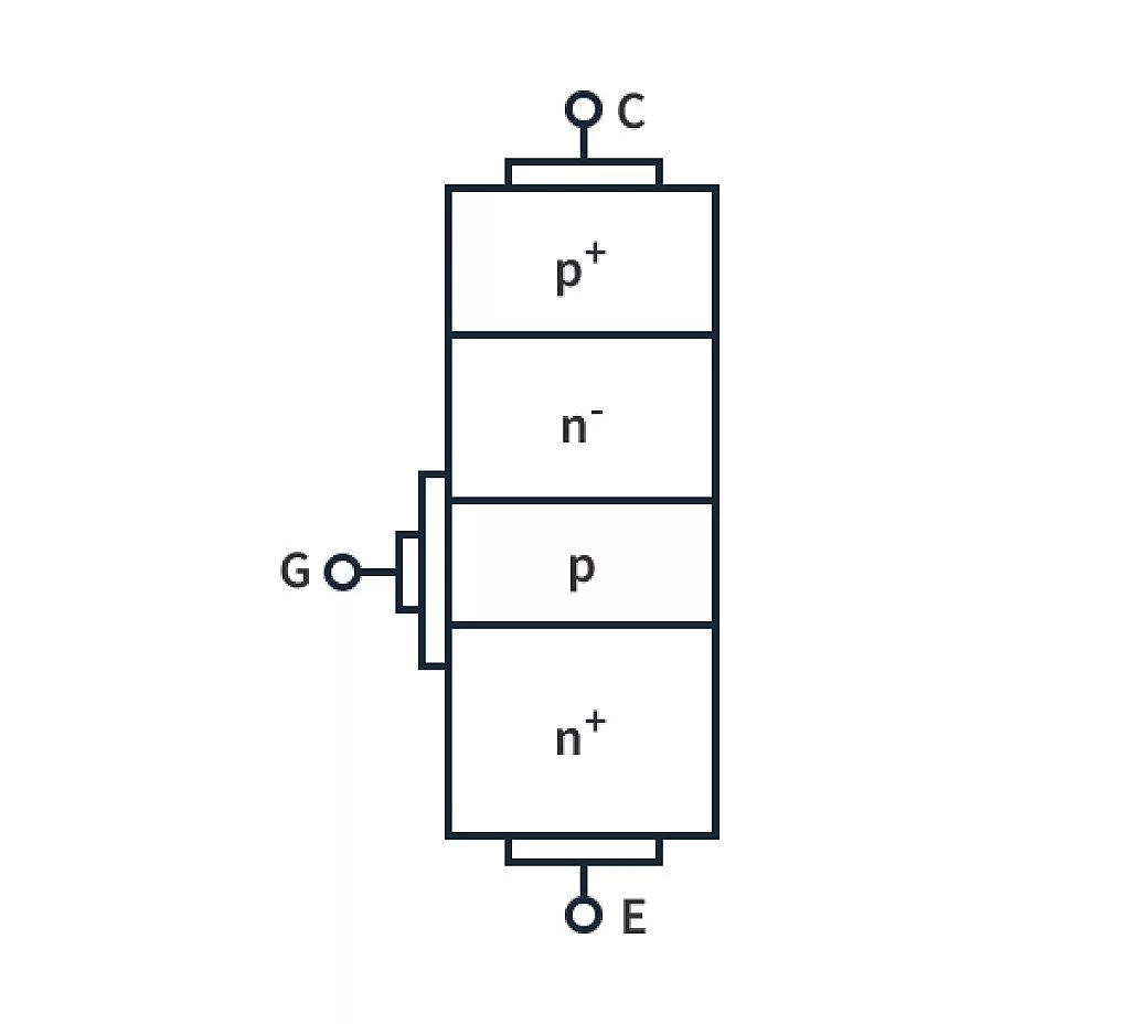
The n-channel IGBT’s semiconductor structure is as shown in the image below.
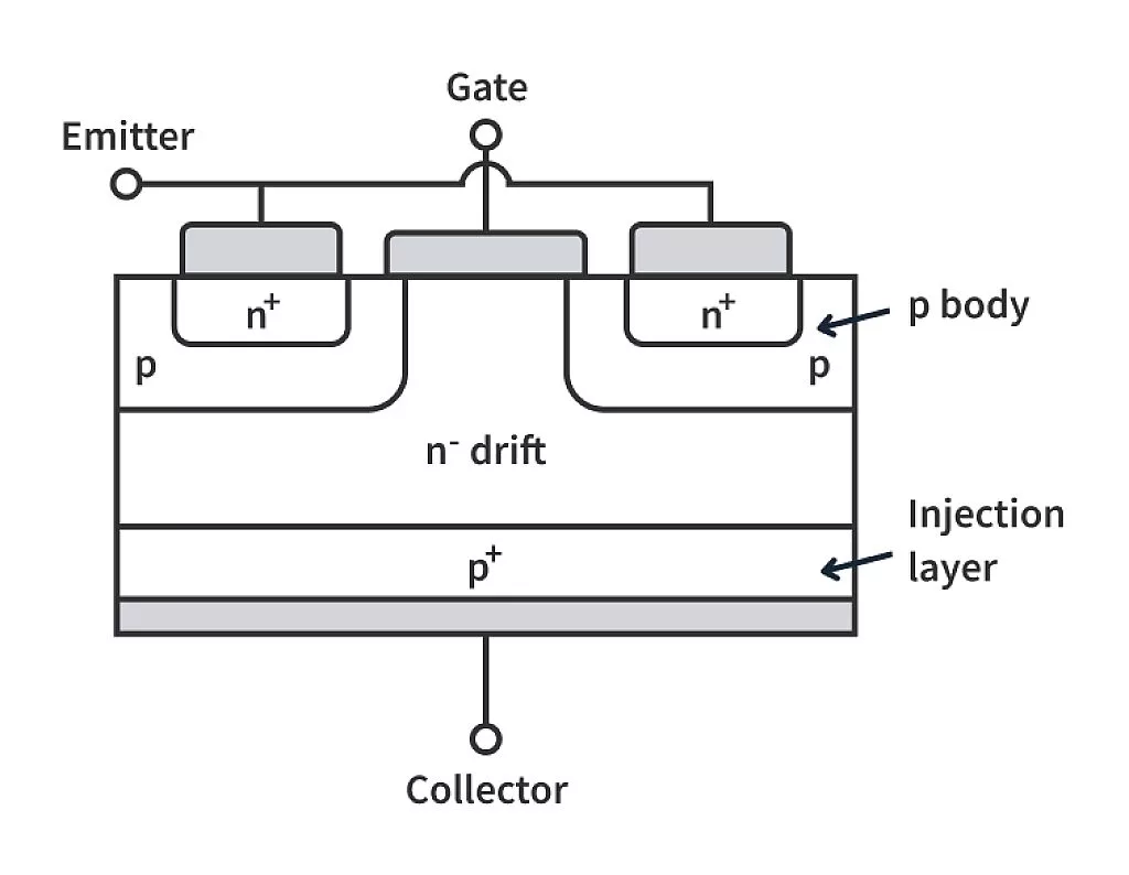
The whole structure is developed on an n-type substrate (specifically, n-type substrate – about which we’ll discuss soon). Two p-bodies are formed at the top. Two n+ wells are created inside the p-body to form the emitter terminal. The n-channel for current conduction is formed with the help of the gate at the top. A superscript of ‘+’ or ‘-’ denotes the doping concentration, with a ‘+’ indicating heavily doped and ‘-’ being lightly doped. The n- layer in the center is a very important layer. This is known as the drift layer. The advantages of a drift layer (lightly doped n layer) have been discussed in detail in the EEFAQ - What is the difference between a normal semiconductor device and a power semiconductor device?
When we talk about the voltage rating of a device, we are talking about the amount of reverse bias the device can handle without breaking down. The n- drift layer increases this voltage rating of the device. For the understanding of this particular EEFAQ, you have to remember that when you dope either the p side or n side or both p and n sides of the pn junction very lightly, the voltage at which the breakdown of the junction occurs under reverse bias increases significantly allowing us to increase the voltage rating of the device. Similarly, when the doping is very high on a junction, that junction breaks down easily. The base-emitter junction of a BJT breaks down easily for this very reason, as the emitter is highly doped. Hence the voltage rating of the BJT is poor. Again, check out the EEFAQ comparing the doping levels to understand the drift layer better.
Returning to the device structure, a p+ injection layer is fabricated at the very end of the wafer forming the collector terminal. It’s called an injection layer because it injects charge carriers (holes) into the n- drift layer to boost current flow in the overall device.
Now that we’ve covered the structure of the IGBT, let's discuss the device operation at the semiconductor level quickly. Look at the image below. Here, we assume the IGBT has been supplied with a DC power source.
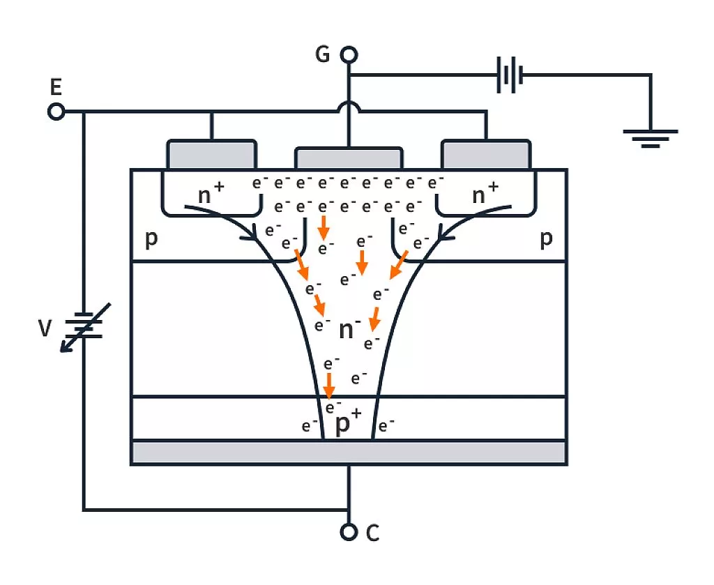
When a positive gate voltage is applied, electrons accumulate under the gate and an n-channel is formed, just like in an NMOS. The p+ layer starts injecting holes into the n- drift layer and in exchange, starts extracting electrons from it. The electrons from the n-channel above start moving into the drift layer to help replenish the electrons lost. Two things happen with this. First, plenty of charge carriers are in the n- layer now, so its resistance decreases. Second, a total pathway of electrons is created - the n-channel is formed between the n+ wells, the p-body, the drift layer, and all the way up to the p+ collector terminal, as shown with the help of the highlight in the image. The arrow marks depict the electron flow; the conventional current hence will be in the opposite direction. A low resistance path for current flow is established, and the device readily supplies current. This was the semiconductor wafer level operation. Let’s simplify the IGBT on the device side and see if we can make anything of it.
This device can be simplified as a pnpn sandwich structure.
If we break the sandwich at around half the n- drift layer, we can see that the device is similar to a PN junction diode in series with an n-channel MOSFET.
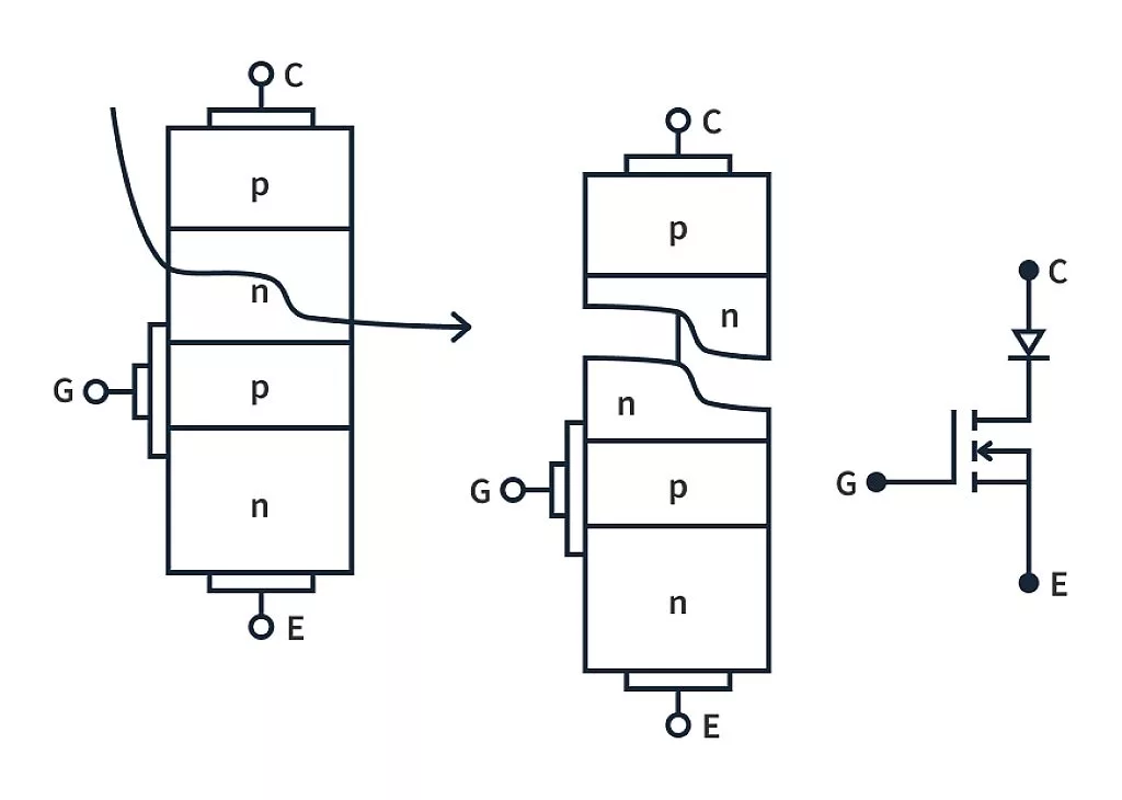
If you’ve studied devices of the transistor family, you know that the BJT breaks down for a negative voltage applied across its collector and emitter terminal. This is because the base-emitter junction, when reverse biased, breaks down easily due to the heavy doping of the emitter. A similar breakdown occurs in MOSFETs as the n wells are highly doped(n+). However, from the equivalent circuit, we can see that the pn junction diode will block the negative voltage across the device’s channel and, additionally, does not break down easily due to the n- drift layer.
This is where the first advantage comes in - the IGBT doesn’t break down as easily or at as low of reverse voltage compared to a BJT or MOSFET and hence can be used in higher voltage rating applications.
Another drawback of the BJT was the base current and the low input impedance of the BJT. With a gate terminal being used in IGBT instead, the control current is minimized to almost 0 (on the order of pico-amperes), and the device’s input impedance is greatly increased. The gate allows for quick turn-off of the IGBT when conducting as well. Removing the gate voltage removes the n-channel under the gate, and a break in the n-channel returns the device current to 0. Again, another advantage over BJT.
Characteristics of IGBT
The operating characteristics of the IGBT are similar to both MOSFET and BJT. Let’s see how.
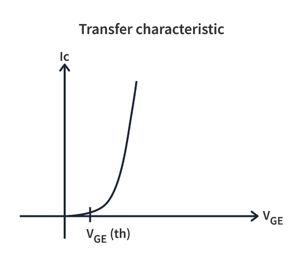
Coming to the transfer characteristics, you’ll find it very similar to that of a MOSFET. The VGE (th) is similar to the threshold voltage in a MOSFET. And once we increase the voltage more than the threshold voltage, iC increases like in a MOSFET.
The static characteristics of the IGBT are similar to that of BJTs.
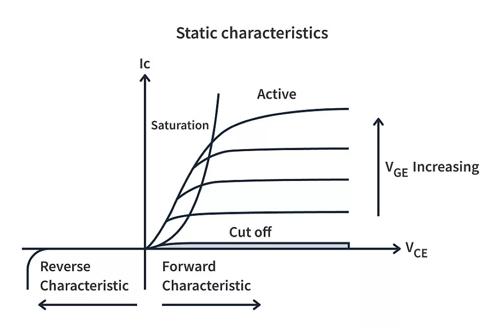
The MOSFET is the faster switch, operating in the nanoseconds range, while the IGBT takes a few 100 nanoseconds. However, this is still suitable for high-power applications like switching amplifiers and industrial control systems and IGBTs are more resilient in high-voltage applications. This is why IGBTs are the preferred choice in traction equipment for electric cars and trains. While they are relatively new compared to MOSFETs and BJTs, IGBTs are here to stay due to that special combination of relatively-fast switching speed and high voltage threshold.
