Communicating with a PC using UART - Part 11 Microcontroller Basics (PIC10F200)
Published
Note: Microchip recently made some changes and their newer IDE versions use the XC8 compiler for Assembly, whereas all sample code here is created for the MPASM compiler. However, the sample code has been ported to XC8 by user tinyelect on our Discord channel (to whom we are extremely grateful!) and the XC8 version of the code is at the bottom of this tutorial for your reference. To see the changes needed to switch from MPASM to XC8, please check out the process that he shared.
Hello again! This time we will try to establish the connection between the PIC10F200 microcontroller and a typical personal computer. Obviously, we can’t connect it to the PC directly (well, several years ago we could, using the LPT port, but now it’s a legacy item and not available in modern PCs). So we will use the USB port of the PC, and we will need a converter to translate the data between the PIC10F200 and USB port.
The most widespread microcontroller interface to communicate with the PC is the UART (Universal Asynchronous Receiver-Transmitter). Also, there are plenty of USB-to-UART converters. The most widespread are based on FT232, CP2102, or CH340 chips. The first one is the most advanced but also the most expensive, while the CH340 is extremely cheap (you can buy a ready-to-use converter board for less than a buck on Aliexpress) and still quite good. Personally I will use the CH340-based board, and you can use whichever you want.
Let’s first consider the UART interface in more detail. I will give just the basics required to understand what and why we made things in this way, and if you need more information you can find it on the Internet, i.e. here. This interface uses up to eight lines to communicate but the minimum required number of lines is just two. The rest are “service lines” and are used for hardware flow control. The mandatory two lines are called Rx and Tx (receive and transmit respectively), and we will use only them in our application. The connection schematic is very simple and is shown in figure 1.

As you can see, only three wires are required - two for the signals, and one for connecting the devices’ ground. Please note that the signal lines are crossed, so the Tx of one device is connected with the Rx of another one and vice versa.
The UART interface is called “asynchronous” because there is no synchronization signal like in SPI or I2C interfaces. A synchronization signal is the sequence of pulses on rising (or falling) edges of which the data is read (or written) from the data lines. This makes the communication determinative as you know exactly which moments you need to read (write) the data.
But how do we exchange data in a determinative way without this signal? In this case, the two devices should first agree about the communication speed and both work with the selected speed. With UART, this communication speed is called the baud rate and the unit of the measure of the symbol rate called “baud”. There are some standard baud rates which came from the times when the UART interface was used by modems (remember those? Before broadband was a thing?). The most widespread baud rates are 1200, 2400, 9600, 19200, 38400, 115200 bauds per second. We will use the value of 9600 because it’s quite high to send short messages without a noticeable delay, and low enough to be emulated by the PIC10F200 microcontroller.
The other feature of the UART interface is that both communicating devices are even, meaning there are no Master and Slave devices and each device can start transmission whenever it needs. The only limitation is that some devices can’t transmit and receive the data simultaneously (like our PIC10F200), in this case we say that communication is half-duplex and you need to take action to prevent attempts at concurrent communication.
Now let’s talk about how the data is sent via the UART interface. First, and it seems to be obvious, the UART is a serial protocol, which means that the data is sent bit by bit via the single line (unlike parallel protocols where the data is sent via several lines simultaneously). Second, the data is normally sent with the least significant bit first. This means that the first one is bit 0, then bit 1, then bit 2 and so on until bit 7. And third, there are special auxiliary bits (basically, communication overhead) that are inserted into the packet and serve special purposes. These bits are:
- Start bit. While idle, the lines of the UART are held high. The start bit, which is always ‘0’, indicates that there is the beginning of the packet.
- Right after the start bit, the eight bits of the transmitted byte are sent, known as the “payload byte”.
- After the payload byte, there might be an “Parity bit” which isn’t absolutely necessary. It is used as a preliminary check to see if the received packet is what was sent. We will skip it, so if you want to know more about it please read here.
- The last one is the Stop bit which is mandatory and is always a ‘1’. After this bit the package is considered to be received and can be processed.
So the minimum length of the UART package is 10 bits: Start bit + Data byte + Stop bit (see figure 2).

Now, as we have the most basic knowledge of the UART interface, we can formulate today’s task. Establish communication between the PC and the PIC10F200 microcontroller via the UART interface. When a button attached to the microcontroller is pressed, we will send the message “Hello” to the PC. When the PIC10F200 receives a ‘1’ from the PC, light on the LED; when it receives a ‘0’, turn off the LED. Ignore everything else.
According to the task, we need to use the PIC10F200 microcontroller (obviously), one LED, one button, and a USB-to-UART converter (as I mentioned before, you can use whichever you want). The new schematics diagram is shown in figure 3.

As you can see in figure 3, the button SW1 is connected to the GP3 pin without any resistors. We can do this because GP3 can never be an output. You should be careful during the device programming though, not to press the switch, otherwise you will short 12V and GND which will not be good for your programmer. If in doubt, better to add the resistor in series to SW1. The LED HL1 is connected to the GP0 pin. The X2 socket represents the USB-to-UART converter. I intentionally didn’t write the pins numbers of the X2 socket as you may have different ones than me. So the Rx pin of the converter is connected to the GP2, which means that we will transmit data to the PC via the GP2 pin. And Tx of the converter is connected to the GP1, thus GP1 is the Rx pin of the microcontroller. That’s all about the schematic, let’s now see how to implement the task in the program.
#include "p10f200.inc"
	__CONFIG _WDT_OFF & _CP_OFF & _MCLRE_OFF

i   		 EQU 10   	 ;Delay register 1
j   		 EQU 11   	 ;Delay register 2
rx_data      EQU 12   	 ;Received byte
tx_data   	 EQU 13   	 ;Byte to transmit
count   	 EQU 14   	 ;Bit counter for UART communication

	ORG 0x0000
INIT
	MOVLW ~((1<<T0CS)|(1<<NOT_GPPU))
	OPTION   		     ;Enable GP2 and pull-ups
	MOVLW ~((1 << GP0) | (1 << GP2))
	TRIS GPIO   		 ;Set GP0 and GP2 as outputs
	BSF GPIO, GP2   	 ;Set GP2 as output high
LOOP
	BTFSC GPIO, GP3  	 ;Check if GP3 is 0 (SW1 is pressed)
	GOTO WAIT_RX    	 ;If it is not 0 then return
	CALL DEBOUNCE_DELAY  ;Otherwise perform the debounce delay
	BTFSC GPIO, GP3    	 ;And check GP3 again
	GOTO WAIT_RX      	 ;If it is not 0 then return
	BTFSS GPIO, GP3    	 ;Otherwise wait while GP3 is 0
	GOTO $-1  	         ;Loop to wait
	CALL DEBOUNCE_DELAY  ;After GP3 is set (SW1 is released)
SEND_MESSAGE    		 ;Start of the sending message via UART
	MOVLW 'H'   		 ;Load the character to send
	CALL TX_BYTE    	 ;And call 'TX_BYTE' subroutine
	MOVLW 'e'            ;Quote marks means use ASCII equivalent
	CALL TX_BYTE
	MOVLW 'l'
	CALL TX_BYTE
	MOVLW 'l'
	CALL TX_BYTE
	MOVLW 'o'
	CALL TX_BYTE
	MOVLW '\r'
	CALL TX_BYTE
	MOVLW '\n'
	CALL TX_BYTE
WAIT_RX
	BTFSS GPIO, GP1     ;Check the GP1 level, if 1 then skip next line
	CALL RX_BYTE   	 ;Otherwise receive the byte
	GOTO LOOP   	;Return to the 'LOOP' label
;--------------------------------------------------------------
TX_BYTE
    MOVWF tx_data   	 ;into the 'tx_data' register
    CLRF count   		 ;Clear the 'count' register
    BCF GPIO, GP2   	             ;Beginning of the Start bit
    CALL UART_DELAY   	 ;One bit delay
SHIFT_TX_DATA   		 ;Start to shift the data byte
    BTFSC tx_data, 0                ;if the LSB of the 'tx_data' is 0
    GOTO SET_BIT   	              ;then skip this line,
    BCF GPIO, GP2   	              ;clear the GP2 bit
    GOTO DELAY   		 ;and go to the 'DELAY' label
SET_BIT   			 ;If the LSB of the 'tx_data' is 1
    BSF GPIO, GP2   	             ;then set the GP2 bit
DELAY
    CALL UART_DELAY   	 ;and perform one bit delay
    RRF tx_data, F   	             ;Shift the data byte to the one bit right
    INCF count, F   	             ;Increment the 'count' register
    BTFSS count, 3   	             ;Check if the third bit of the 'count' is 1 (count = 8)
    GOTO SHIFT_TX_DATA    ;If it is not set then return to the 'SHIFT_TX_DATA'
    BSF GPIO, GP2   	            ;Otherwise start the Stop bit
    CALL UART_DELAY           ;and perform one bit delay
    RETLW 0
;--------------------------------------------------------------
RX_BYTE   			 ;Beginning of the RX_BYTE subroutine
    CALL HALF_UART_DELAY;Delay to the middle of the bit interval
    BTFSC GPIO, GP1   	 ;If the GP1 bit is not 0
    RETLW 0   			 ;then error of the Start bit, and return
    CLRF count   		 ;Else clear 'count' register
    CLRF rx_data   	             ;and clear 'rx_data' register
SHIFT_RX_DATA   		 ;Start receiving the data byte
    CALL UART_DELAY            ;Call one bit delay
    RRF rx_data, F   	              ;Shift the 'rx_data' one bit to the right
    BTFSC GPIO,GP1   	 ;If GP1 bit is 1
    BSF rx_data, 7   	              ;then set the MSB of the 'rx_data' to 1
    INCF count, F   	              ;Increment the counter
    BTFSS count, 3   	              ;and check if it is 8
    GOTO SHIFT_RX_DATA    ;If it is not then return to the 'SHIFT_RX_DATA'
    CALL UART_DELAY            ;Otherwise call one bit delay
    BTFSS GPIO, GP1   	 ;And check the stop bit
    RETLW 0   			 ;if the GP1 is not 1 then return
    MOVLW '1'   		 ;Else load the '1' into the W register
    XORWF rx_data, W             ;And perform the XOR between W and 'rx_data'
    BTFSC STATUS, Z   	 ;If result is 0 (rx_data = W)
    BSF GPIO, GP0   	              ;then set the GP0 bit
    MOVLW '0'   		 ;Make the same check for the '0' value
    XORWF rx_data, W
    BTFSC STATUS, Z
    BCF GPIO, GP0   	             ;and clear the GP0 bit if rx_data = '0'
    RETLW 0
;--------------------------------------------------------------
UART_DELAY  	     	 ;Start UART_DELAY subroutine here
	MOVLW D'29'  	 ;Load initial value for the delay
	MOVWF i  		;Copy the value to the register i
DELAY_LOOP_UART   	 ;Start delay loop
	DECFSZ i, F  		 ;Decrement i and check if it is not zero
	GOTO DELAY_LOOP_UART;If not, go to the DELAY_LOOP_UART label
	RETLW 0  		;Else return from the subroutine

HALF_UART_DELAY 		 ;Start HALF_UART_DELAY subroutine here

	MOVLW D'16'  	 ;Load initial value for the delay
	MOVWF i  		 ;Copy the value to the register i
DELAY_LOOP_HALF   	 ;Start delay loop
	DECFSZ i, F  		 ;Decrement i and check if it is not zero
	GOTO DELAY_LOOP_HALF;If not, go to the DELAY_LOOP_HALF label
	RETLW 0  		;Else return from the subroutine

DEBOUNCE_DELAY  	  ;Start DEBOUNCE_DELAY subroutine here
	MOVLW D'40'  	 ;Load initial value for the delay
	MOVWF i  		 ;Copy the value to the register i
	MOVWF j  		  ;Copy the value to the register j
DELAY_LOOP  		 ;Start delay loop
	DECFSZ i, F  		 ;Decrement i and check if it is not zero
	GOTO DELAY_LOOP  ;If not, then go to the DELAY_LOOP label
	DECFSZ j, F  		 ;Decrement j and check if it is not zero
	GOTO DELAY_LOOP  ;If not, then go to the DELAY_LOOP label
	RETLW 0  		 ;Else return from the subroutine

	END
The program seems to be long but in fact there are a lot of repeating and familiar parts so I believe we will review it quite fast.
First, in lines 4 and 5, we define two registers ‘i’ and ‘j’ to be used for delay purposes. Then, in line 6 we define the ‘rx_data’ register into which we will be receiving the incoming byte from the PC and ‘tx_data’ in line 7 to load the byte to be transmitted to the PC into it. And finally, in line 8, we define the ‘count’ register which will be used as a bits counter while data shift during the reception/transmission.
The initialization part in lines 11-16 doesn't consist of anything new. We configure the GP2 pin as a GPIO, enable the pull-up resistors on the input pins (lines 12-13). Then configure the GP0 and GP2 pins as outputs (lines 14-15) and finally set the GP2 pin high (line 16). As a reminder, GP2 is the Tx pin of the microcontroller, and we are responsible to keep it high in the idle state.
	BTFSC GPIO, GP3  	 ;Check if GP3 is 0 (SW1 is pressed)
	GOTO WAIT_RX    	 ;If it is not 0 then return
	CALL DEBOUNCE_DELAY  ;Otherwise perform the debounce delay
	BTFSC GPIO, GP3    	 ;And check GP3 again
	GOTO WAIT_RX      	 ;If it is not 0 then return
	BTFSS GPIO, GP3    	 ;Otherwise wait while GP3 is 0
	GOTO $-1  	         ;Loop to wait
	CALL DEBOUNCE_DELAY  ;After GP3 is set (SW1 is released)
In lines 18-25 we check to see if button SW1 is pressed. We did the same in Tutorial 9, so I will not pause here. The main difference is that there we made the checking in the subroutine, and here we make it in the main loop. This is because of the stack limitation. We can’t call 2 nested subroutines, unfortunately. If you don’t remember why, I recommend reviewing some of the first tutorials - they’ll probably make more sense this time around anyway. Because of this implementation if the button is not pressed, we use GOTO WAIT_RX instruction instead of RETLW 0. ‘WAIT_RX’ stands for waiting to receive the byte part of the program which starts at line 55.
SEND_MESSAGE    	 ;Start of the sending message via UART
	MOVLW 'H'   	 ;Load the character to send
	CALL TX_BYTE     ;And call 'TX_BYTE' subroutine
	MOVLW 'e'        ;Quote marks means use ASCII equivalent
	CALL TX_BYTE
	MOVLW 'l'
	CALL TX_BYTE
	MOVLW 'l'
	CALL TX_BYTE
	MOVLW 'o'
	CALL TX_BYTE
	MOVLW '\r'
	CALL TX_BYTE
	MOVLW '\n'
	CALL TX_BYTE
WAIT_RX
	BTFSS GPIO, GP1  ;Check the GP1 level, if 1 then skip next line
	CALL RX_BYTE   	 ;Otherwise receive the byte
	GOTO LOOP   	 ;Return to the 'LOOP' label
If the button has been pressed we finally get to line 26 which is marked with the label ‘SEND_MESSAGE’. It consists of repeating blocks 2 lines each. So we will consider only one block in detail.
In line 27 we load the value ‘H’ into the W register by means of the MOVLW instruction. Please note that using a literal this way is also acceptable. You can load any ASCII symbol using the single quotes. In this case we load the ‘H’ character.
In line 28 we call the ‘TX_BYTE’ subroutine where the loaded character is transmitted via the UART.
In the same way we load consequent characters ‘H’, ‘e’, ‘l’, ‘l’, ‘o’, ‘\r’, and ‘\n’. Probably the last two characters aren’t as clear for you. ‘\r’ is very different from ‘r’ as the last one is just the ‘r’ character while the first one stands for the Carriage Return (CR) character which has ASCII code 13. ‘\n’ stands for the Line Feed (LF) character which has ASCII code 10. These two characters are used as the line terminator and often are called CRLF, or CR+LF.
So the message we send will print the world “Hello” and start a new line.
TX_BYTE
    MOVWF tx_data   	 ;into the 'tx_data' register
    CLRF count   		 ;Clear the 'count' register
    BCF GPIO, GP2   	 ;Beginning of the Start bit
    CALL UART_DELAY   	 ;One bit delay
Let’s now move to line 46 where the ‘TX_BYTE’ subroutine starts. In this subroutine we implement the transmission of one UART packet including Start, Stop bits and Data byte.
First, we copy the data byte from W register into the ‘tx_data’ register (line 47). Then we clear the ‘count’ register (line 48). Now we are ready for transmission.
First we need to send the Start bit. To do this we set the GP2 pin low (line 49) and wait for the specified time by calling the ‘UART_DELAY’ subroutine (line 50).
What is this specified time? As we agreed earlier, we use the speed rate of 9600 baud, or 9600 bits per second. Which means that each bit has the duration of 1/9600 = 0.000104s = 104us. Thus the ‘UART_DELAY’ subroutine performs this delay. It is located in lines 95-101.
UART_DELAY  	     	 ;Start UART_DELAY subroutine here
	MOVLW D'29'  	     ;Load initial value for the delay
	MOVWF i  		     ;Copy the value to the register i
DELAY_LOOP_UART   	     ;Start delay loop
	DECFSZ i, F  		 ;Decrement i and check if it is not zero
	GOTO DELAY_LOOP_UART ;If not, go to the DELAY_LOOP_UART label
	RETLW 0  		     ;Else return from the subroutine
It’s the typical delay using only one register and with an initial value of 29.
Please note that due to the difference of the clock frequency of different microcontrollers, this value also may differ. You probably will need to change it before you get stable communication.
But let’s return to the transmission procedure. After we transmit the Start bit we can now transmit the Data byte. This operation is performed in lines 51-63.
SHIFT_TX_DATA   		 ;Start to shift the data byte
    BTFSC tx_data, 0     ;if the LSB of the 'tx_data' is 0
    GOTO SET_BIT   	     ;then skip this line,
    BCF GPIO, GP2   	 ;clear the GP2 bit
    GOTO DELAY   		 ;and go to the 'DELAY' label
SET_BIT   			     ;If the LSB of the 'tx_data' is 1
    BSF GPIO, GP2   	 ;then set the GP2 bit
DELAY
    CALL UART_DELAY   	 ;and perform one bit delay
    RRF tx_data, F   	 ;Shift the data byte to the one bit right
    INCF count, F   	 ;Increment the 'count' register
    BTFSS count, 3   	 ;Check if the third bit of the 'count' is 1 (count = 8)
    GOTO SHIFT_TX_DATA   ;If it is not set then return to the 'SHIFT_TX_DATA'
Line 51 is just a label ‘SHIFT_TX_DATA’ which indicates that here starts the shift of data to start transmitting it bitwise.
First, we check the LSB of the ‘tx_data’ register (line 52). If it is 0, then line 53 is skipped and line 54 is implemented where the GP2 pin is set low by means of the BCF instruction. Then we move to line 58 using the GOTO instruction to skip lines 56-57.
If the LSB of the ‘tx_data’ is 1 then line 53 is implemented and we move to line 56 by means of the GOTO instruction. In line 56 there is just a label ‘SET_BIT’, and the action is implemented in line 57 where GP2 pin is set high using the BSF instruction.
After GP2 pin is set high or low depending on the LSB of the ‘tx_data’ we get to line 58 where we have the ‘DELAY’ label. In line 59 we call the ‘UART_DELAY’ subroutine once again to wait for one more bit interval.
After that we shift the ‘tx_data’ one bit to the right using the RRF instruction (line 60), and now we are ready to check bit #1.
In line 61 we increment the ‘count’ register, and in line 62 we check the third bit of this register. We already used a similar trick in tutorial 10. If the third bit of the ‘count’ register is set, it means that we reached the value 8 (‘1000’ in binary), and all eight bits of the data byte have been transmitted. If the third bit of the ‘count’ register is not set yet, line 63 is not skipped and we move to the label ‘SHIFT_TX_DATA’ (line 51) to send the next bit.
    GOTO SHIFT_TX_DATA    ;If it is not set then return to the 'SHIFT_TX_DATA'
    BSF GPIO, GP2   	  ;Otherwise start the Stop bit
    CALL UART_DELAY       ;and perform one bit delay
    RETLW 0
And if this bit is finally set, then line 63 is skipped, and we move to line 64 where we set the GP2 pin high starting the Stop bit. Then we perform the specified ‘UART_DELAY’ once again (line 65) and leave the subroutine (line 66).
As you can see there is nothing complex here. We even didn’t use any new instructions or approaches - you already knew everything needed to do this.
WAIT_RX
	BTFSS GPIO, GP1  ;Check the GP1 level, if 1 then skip next line
	CALL RX_BYTE   	 ;Otherwise receive the byte
	GOTO LOOP   	 ;Return to the 'LOOP' label
Now let’s consider how the byte reception is implemented, and return to line 41 for this.
In line 41 there is the ‘WAIT_RX’ label, it indicates that here we wait for some activity on the GP1 pin which plays the role of the Rx line of the microcontroller.
In line 42 we check if GP1 pin is high. If it is, (which means that the Rx line is idle) then line 43 is skipped and we go to line 44 where we meet the GOTO LOOP instruction which returns us to the beginning of the main loop where we check the button state again.
And if GP1 pin is low (which means that the PC has sent Start bit) then line 43 is implemented, and we call the ‘RX_BYTE’ subroutine, in which (as you can assume from its title) we receive the byte from the PC.
RX_BYTE   			     ;Beginning of the RX_BYTE subroutine
    CALL HALF_UART_DELAY ;Delay to the middle of the bit interval
    BTFSC GPIO, GP1   	 ;If the GP1 bit is not 0
    RETLW 0   			 ;then error of the Start bit, and return
    CLRF count   		 ;Else clear 'count' register
    CLRF rx_data   	     ;and clear 'rx_data' register
Let’s now move to line 68 where this subroutine starts and see how it’s implemented. Actually it’s very similar to the TX_BYTE subroutine which is not surprising because the packet has the same structure. But there are some certain differences in receiving the byte in comparison to the transmitting.
Firstly, in line 69 we call the ‘HALF_UART_DELAY’ subroutine. This subroutine is the same as the ‘UART_DELAY’ and differs only with the initialization value (line 104). Why do we need this? We call the ‘RX_BYTE’ subroutine right after we detect the beginning of the Start bit. and if we will check the incoming bits with the period defined by ‘UART_DELAY’ it can happen that we check the same bit twice or skip some bit because the data rates are not equal. For instance the actual baud rate of the USB-to-UART converter is 9550 bps, and the actual baud rate of the PIC10F200 is 9650 bps. We have a difference which will cause a small time shift at each bit, and finally lead to the situation that the last bit is skipped entirely.
That’s why it’s good practice to check the incoming data in the middle of the bit interval. In this case, even if there is a deviation from the baud rate we will receive the entire packet of data correctly. You may notice that I set the initial value of half delay as 16, not 14 or 15 which is half of 29. I set it experimentally, because with the smaller values the reception was not stable. So you will also need to adjust the value at line 104 until you get a stable result.
Well, now we are in the middle of the bit interval, and we remember that this should be the Start bit. We need to make sure that this is really the Start bit and not some random pulse. That’s why we check if GP1 is still 0 (line 70). If it is not 0 then line 71 is not skipped and we return from the subroutine. If it’s still 0 then we have a hope that we can get some data. In this case we move to line 72 where we clear the ‘count’ register to prepare it for the byte reception, and then to line 73 where we clear ‘rx_data’ register for the same reason.
SHIFT_RX_DATA   		 ;Start receiving the data byte
    CALL UART_DELAY      ;Call one bit delay
    RRF rx_data, F   	 ;Shift the 'rx_data' one bit to the right
    BTFSC GPIO,GP1   	 ;If GP1 bit is 1
    BSF rx_data, 7   	 ;then set the MSB of the 'rx_data' to 1
Line 74 tells us that here ‘SHIFT_RX_DATA’ starts which is very similar to the ‘TX_DATA’, as I already mentioned.
In line 75 we call the ‘UART_DELAY’ subroutine. Now we don’t need to move half intervals anymore.
In line 76 we shift the ‘rx_data’ register one bit to the right. We make it here before checking the incoming data on purpose. If we shift the register after checking the data, we will make one more shift after the last received bit and thus the MSB will become LSB (remember that our shifting command rotates all the way around) which we don’t need. And if we shift the register here, everything will be OK, and this first extra shift doesn’t mess with anything as ‘rx_data’ has all zeros anyway.
Then we check the GP1 pin (line 77). If it is 1 then line 78 is implemented, and we set the MSB of the ‘rx_data’ register as 1. Why do we set the MSB if we remember that the data comes LSB first? It’s quite easy. Let’s imagine what’s going on there. We receive the first bit and load it into the MSB, then we shift the register to the right, and this bit becomes #6, after the second shift it will be #5 and so on. So after all 7 shifts it will become the LSB which is what we need.
If the GP1 pin is 0, we just skip line 78 and add nothing. This makes sense because we cleared the ‘rx_data’ register first, and now there is no reason to set the bit to zero, as it’s already zero.
    INCF count, F   	  ;Increment the counter
    BTFSS count, 3   	  ;and check if it is 8
    GOTO SHIFT_RX_DATA    ;If it is not then return to the 'SHIFT_RX_DATA'
    INCF count, F   	  ;Increment the 'count' register
    BTFSS count, 3   	  ;Check if the third bit of the 'count' is 1 (count = 8)
    GOTO SHIFT_TX_DATA    ;If it is not set then return to the 'SHIFT_TX_DATA'
Lines 79-81 are the same as lines 61-63 of the ‘TX_BYTE’. We increment the ‘count’ and check the third bit to figure out if we have received all eight bits. If not we move to the label ‘SHIFT_RX_DATA’ (line 81), and if so, then this line is skipped, and we proceed further.
    CALL UART_DELAY      ;Otherwise call one bit delay
    BTFSS GPIO, GP1   	 ;And check the stop bit
    RETLW 0   			 ;if the GP1 is not 1 then return
    MOVLW '1'   		 ;Else load the '1' into the W register
    XORWF rx_data, W     ;And perform the XOR between W and 'rx_data'
    BTFSC STATUS, Z   	 ;If result is 0 (rx_data = W)
    BSF GPIO, GP0   	 ;then set the GP0 bit
    MOVLW '0'   		 ;Make the same check for the '0' value
    XORWF rx_data, W
    BTFSC STATUS, Z
    BCF GPIO, GP0   	 ;and clear the GP0 bit if rx_data = '0'
    RETLW 0
In line 82, we call the ‘UART_DELAY’ once again to check the Stop bit. If GP1 pin is high (line 83) during the Stop bit (which is correct) then line 84 is skipped, and we move to checking the received byte. In the other case, we return from the subroutine as there is a Stop bit error (line 84).
In line 85 we load the value ‘1’ into the W register. Please be attentive: ‘1’ and 1 are very different values. 1 is just a number while ‘1’ is the ASCII character representing the 1, and its value is 49. As we will send the data via some terminal program in the ASCII format it’s important to check the incoming data as characters, not just numbers.
In line 86 we perform the exclusive OR (XOR) operation between the ‘rx_data’ and W. This is a trick to check if the values are equal. As you hopefully remember, if we perform the XOR operation between equal values (whether they’re both zeros or both ones) the result will be zero. And if there is difference in at least one bit the overall result will differ from zero. We can use this feature to check the equality of two values.
So if the incoming byte was ‘1’ then the result of the XOR operation will be 0, and the Z bit of the STATUS register will be set. We check this in line 87. If it was set (‘rx_data’ = ‘1’) then line 88 is not skipped and the GP0 pin is set high.
In lines 89-92 we perform the same check but for the value ‘0’. And if ‘rx_data’ = ‘0’ then GP0 is set low (line 92).
Well, that’s about it for the program. As you see, there is nothing hard in either the transmission or in reception via UART.
So let’s assemble the device, load the program and try to work with it.
First, I want to show you how the real UART data looks. As I mentioned in one of the earlier tutorials, there is such a cool thing called a Logic analyzer. If you connect it to the GP2 pin you can see the actual signals and even decode the UART packet (see figure 4).

Here you can see how the voltage level is changed. The blue rectangles above are the decoded characters, and you may notice that we have here exactly what we sent. The payload bits are marked with the dots. The low interval before the first dot of each byte is the Start bit, and the high interval after the last dot is the Stop bit. You also may notice that some dots are very close to the voltage change edges. This happens because of the deviation from the data rate from the specified one (which I was talking about earlier).
If you have a tool like this, it’s quite easy to check the communication and to correct the delay values to get the best results.
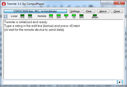
But let’s now try to communicate with the PC. In addition to the USB-to-UART converter you also need some terminal program to work with the COM port. There are plenty of them, and I won’t advise you on this, you can select the one which is the most convenient for you. I will show you how to establish communication using the Termite program.
After you run the program you will see the following window:
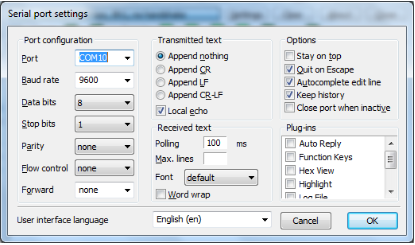
Press ‘Settings’ button to set the correct settings:
First you need to select the correct port. When you connect your USB-to-UART converter it will be recognized by the system as a COM port. You need to check its number using the Device Manager:
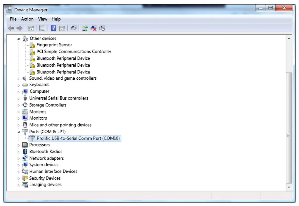
As you can see, my port number is 10 and I set this port in the settings of the Termite. Also I set the Baud rate as 9600, data bits as 8, Stop bits as 1, Parity and Flow control as ‘none’. Also, in the next column it’s better to select ‘Append nothing’ in the ‘Transmitted text’ block. And then press OK. Now we are ready to work.
Let’s press the button on the device a couple times and see what we will receive:
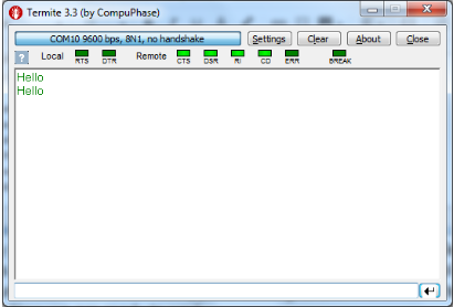
As you see, we get the Hello text twice, and the next one starts with the new line due to CRLF combination sent.
Now let’s enter 1 in the bottom line and press Enter. You should see that the LED is now on. If it didn’t happen, correct the value in line 104 to get your timing right. If it did turn on, now enter 0 and press Enter again. You will see that the LED is now turned off. This means everything works as desired.
And finally, some statistics. We didn’t learn any new instructions or registers this time but we learned how to exchange the data using the UART interface. The whole program uses just 89 words.
I also want to mention that in more “mature” microcontrollers there is a hardware UART module which does all these things automatically, you just copy the data to be sent into its shift register, flip a bit, and wait. The same with the reception, it receives the byte, clears it, checks error and notifies you about all these events using interrupts. This is really cool but it hides from us how this everything works, and we now know a bit more - that is a reason to be proud.
Exercise
As homework I’d recommend you to make the following task using the same hardware. Receive the numbers from 0 to 9 from the PC and change the brightness of the LED accordingly, where 0 corresponds to the LED off, and 9 corresponds to the 100% of brightness. And when the button is pressed send the message “Brightness:x”, where x is the number sent before.
Here’s my solution of the suggested homework:
 #include "p10f200.inc"
	__CONFIG _WDT_OFF & _CP_OFF & _MCLRE_OFF

i 		 EQU 10 	 ;Delay register 1
j 		 EQU 11 	 ;Delay register 2
rx_data EQU 12 	 ;Received byte
tx_data 	 EQU 13 	 ;Data to transmit
count 	 EQU 14 	 ;Bit counter for UART communication
limit 	 EQU 15 	 ;PWM limit
pwm_count EQU 16 	 ;PWM counter

	ORG 0x0000
INIT
	MOVLW ~((1<<T0CS)|(1<<NOT_GPPU))
	OPTION 			 ;Enable GP2 and pull-ups
	MOVLW ~((1 << GP0) | (1 << GP2))
	TRIS GPIO 		 ;Set GP0 and GP2 as outputs
 BSF GPIO, GP2 	 ;Set GP2 as output high
LOOP
 MOVF limit, W 	 ;Copy the PWM limit value of the W register
	XORWF pwm_count, W ;Subtract the W from 'pwm_count'
	BTFSS STATUS, Z 	 ;If the result is not 0
	GOTO $ + 2 		 ;then go to the line 25
	BSF GPIO, GP0 	 ;else set the GP0 pin
	DECF pwm_count, F	;Decrement 'pwm_count', check if the result is 0
	BTFSS STATUS, Z 	 ;If the result is not 0
	GOTO CHECK_BUTTON ;then go to CHECK_BUTTON
 MOVLW D'9' 	 ;Set the initial value of 'pwm_count'
	MOVWF pwm_count 	 ;as 9
	BCF GPIO, GP0 		 ;Reset GP0 pin

CHECK_BUTTON
 BTFSC GPIO, GP3 	 ;Check if GP3 is 0 (SW1 is pressed)
	GOTO WAIT_RX 	 ;If it is not 0 then return
	CALL DEBOUNCE_DELAY ;Otherwise perform the debounce delay
	BTFSC GPIO, GP3 	;And check GP3 again
	GOTO WAIT_RX 		 ;If it is not 0 then return
	BTFSS GPIO, GP3 	;Otherwise wait while GP3 is 0
	GOTO $-1 		 ;Loop to wait
	CALL DEBOUNCE_DELAY ;After GP3 is set (SW1 is released)
SEND_MESSAGE 		 ;Start of the sending message via UART
	MOVLW 'B' 		 ;Load the character to send
 CALL TX_BYTE 	 ;And call 'TX_BYTE' subroutine
 MOVLW 'r'
 CALL TX_BYTE
 MOVLW 'i'
 CALL TX_BYTE
 MOVLW 'g'
 CALL TX_BYTE
 MOVLW 'h'
 CALL TX_BYTE
 MOVLW 't'
 CALL TX_BYTE
 MOVLW 'n'
 CALL TX_BYTE
 MOVLW 'e'
 CALL TX_BYTE
 MOVLW 's'
 CALL TX_BYTE
 MOVLW 's'
 CALL TX_BYTE
 MOVLW ':'
 CALL TX_BYTE
 MOVF rx_data, W 	 ;Load the 'rx_data' value
 CALL TX_BYTE 	 ;And call 'TX_BYTE' subroutine
 MOVLW '\r'
 CALL TX_BYTE
 MOVLW '\n'
 CALL TX_BYTE
WAIT_RX
 BTFSS GPIO, GP1 ;Check the GP1 level, if 1 then skip next line
 CALL RX_BYTE 	 ;Otherwise receive the byte
	GOTO LOOP 		 ;Return to the 'LOOP' label
;--------------------------------------------------------------
TX_BYTE
 MOVWF tx_data 	 ;into the 'tx_data' register
 CLRF count 		 ;Clear the 'counr' register
 BCF GPIO, GP2 	 ;Beginning of the Start bit
 CALL UART_DELAY 	 ;One bit delay
SHIFT_TX_DATA 		 ;Shart to shift the data byte
 BTFSC tx_data, 0 ;if the LSB of the 'tx_data' is 0
 GOTO SET_BIT 	 ;then skip this line,
 BCF GPIO, GP2 	 ;clear the GP2 bit
 GOTO DELAY 		 ;and go to the 'DELAY' label
SET_BIT 				 ;If the LSB of the 'tx_data' is 1
 BSF GPIO, GP2 	 ;then set the GP2 bit
DELAY
 CALL UART_DELAY 	 ;and perform one bit delay
 RRF tx_data, F 	 ;Shift the data byte to the one bit right
 INCF count, F 	 ;Increment the 'count' register
 BTFSS count, 3 	 ;Check if the third bit of the 'count' is 1 (count = 8)
 GOTO SHIFT_TX_DATA ;If it is not set then return to the 'SHIFT_TX_DATA'
 BSF GPIO, GP2 	 ;Otherwise start the Stop bit
 CALL UART_DELAY ;and perform one bit delay
 RETLW 0
;--------------------------------------------------------------
RX_BYTE 			 ;Beginning of the RX_BYTE subroutine
 CALL HALF_UART_DELAY;Delay to the middle of the bit interval
 BTFSC GPIO, GP1 	 ;If the GP1 bit is not 0
 RETLW 0 			 ;then error of the Start bit, and return
 CLRF count 		 ;Else clear 'count' register
 CLRF rx_data 	 ;and clear 'rx_data' register
SHIFT_RX_DATA 		 ;Start receiving the data byte
 CALL UART_DELAY ;Call one bit delay
 RRF rx_data, F 	 ;Shift the 'rx_data' noe bit to the right
 BTFSC GPIO,GP1 	 ;If GP1 bit is 1
 BSF rx_data, 7 	 ;then set the MSB of the 'rx_data' to 1
 INCF count, F 	 ;Increment the counter
 BTFSS count, 3 	 ;and check if it is 8
 GOTO SHIFT_RX_DATA ;If it is not then return to the 'SHIFT_RX_DATA'
 CALL UART_DELAY ;Otherwise call one bit delay
 BTFSS GPIO, GP1 	 ;And check the stop bit
 RETLW 0 			 ;if the GP1 is not 1 then return
CHECK_RX_BYTE
 MOVLW '0' 		 ;Load the '0' into the W register
 XORWF rx_data, W ;And perform the XOR between W and 'rx_data'
 BTFSS STATUS, Z 	 ;If result is not 0 (rx_data != W)
 GOTO $+3 		 ;then check the next number
 MOVLW 0 			 ;Otherwise load 0 into W register
 GOTO LOAD 		 ;And go to the LOAD label
 MOVLW '1'
 XORWF rx_data, W
 BTFSS STATUS, Z
 GOTO $+3
 MOVLW 1
 GOTO LOAD
 MOVLW '2'
 XORWF rx_data, W
 BTFSS STATUS, Z
 GOTO $+3
 MOVLW 2
 GOTO LOAD
 MOVLW '3'
 XORWF rx_data, W
 BTFSS STATUS, Z
 GOTO $+3
 MOVLW 3
 GOTO LOAD
 MOVLW '4'
 XORWF rx_data, W
 BTFSS STATUS, Z
 GOTO $+3
 MOVLW 4
 GOTO LOAD
 MOVLW '5'
 XORWF rx_data, W
 BTFSS STATUS, Z
 GOTO $+3
 MOVLW 5
 GOTO LOAD
 MOVLW '6'
 XORWF rx_data, W
 BTFSS STATUS, Z
 GOTO $+3
 MOVLW 6
 GOTO LOAD
 MOVLW '7'
 XORWF rx_data, W
 BTFSS STATUS, Z
 GOTO $+3
 MOVLW 7
 GOTO LOAD
 MOVLW '8'
 XORWF rx_data, W
 BTFSS STATUS, Z
 GOTO $+3
 MOVLW 8
 GOTO LOAD
 MOVLW '9'
 XORWF rx_data, W
 BTFSS STATUS, Z
 GOTO $+3
 MOVLW 9
LOAD
 MOVWF limit 		 ;Copy the W value into the 'limit'
 RETLW 0
;--------------------------------------------------------------
UART_DELAY 	 	 ;Start UART_DELAY subroutine here
	MOVLW D'29' 		 ;Load initial value for the delay
	MOVWF i 			 ;Copy the value to the register i
DELAY_LOOP_UART 	 ;Start delay loop
	DECFSZ i, F 		 ;Decrement i and check if it is not zero
	GOTO DELAY_LOOP_UART;If not, go to the DELAY_LOOP_UART label
	RETLW 0 			 ;Else return from the subroutine

HALF_UART_DELAY 		 ;Start HALF_UART_DELAY subroutine here

	MOVLW D'16' 		 ;Load initial value for the delay
	MOVWF i 			 ;Copy the value to the register i
DELAY_LOOP_HALF 	 ;Start delay loop
	DECFSZ i, F 		 ;Decrement i and check if it is not zero
	GOTO DELAY_LOOP_HALF;If not, go to the DELAY_LOOP_HALF label
	RETLW 0 			 ;Else return from the subroutine

DEBOUNCE_DELAY 	 ;Start DEBOUNCE_DELAY subroutine here
	MOVLW D'40' 		 ;Load initial value for the delay
	MOVWF i 			 ;Copy the value to the register i
	MOVWF j 			 ;Copy the value to the register j
DELAY_LOOP 		 ;Start delay loop
	DECFSZ i, F 		 ;Decrement i and check if it is not zero
	GOTO DELAY_LOOP 	 ;If not, then go to the DELAY_LOOP label
	DECFSZ j, F 		 ;Decrement j and check if it is not zero
	GOTO DELAY_LOOP 	 ;If not, then go to the DELAY_LOOP label
	RETLW 0 			 ;Else return from the subroutine

	END
Download Homework Code
Yeah, I know, it’s a lot longer, nearly double the length. I’ll explain just a few portions.
First, the PWM part. It’s located in lines 20 to 30. It’s quite similar to the one given in tutorial 7. The main differences are:
1. We don’t use any delay here so as not to miss the beginning of the UART packet. We can afford a 10 us delay to execute ten lines of the code, but it’s not good to spend more time.
2. We set the maximum value of the PWM as 9, not as 255 like in Tutorial 7. This is because of the given task: we have just ten grades of the brightness - from 0 to 9, so no need to use 255 grades.
3. We set the output pin low when we set the ‘pwm_count’ as 9, and set the output pin high when the ‘pwm_count’ matches the ‘limit’. This is quite simple. As we decrement the ‘pwm_count’ at every iteration the maximum brightness will be achieved when the ‘limit’ is ‘9’, as the LED will turn on immediately and stay on while ‘pwm_count’ decreases from 9 to 0. And if the ‘limit’ is 0 we never reach the situation when ‘pwm_count’ = ‘limit’ (because as soon as ‘pwm_count’ becomes 0 we set it to 9), thus the LED will stay off all the time (which we need according to the task).
4. We load the initial value into the ‘pwm_count’ register at the end of the PWM part of the code. It’s also OK, after startup we may have some undefined behavior but it will take several milliseconds, so you probably won’t notice it. But we saved a couple lines of code. If you want, you may copy lines 28-30 into the initialization part to calm your conscience.
That’s all about the PWM. Now let’s move to the transmission part.
‘SEND_MESSAGE’ part takes lines 41 to 69. Almost everything is the same in comparison to the initial program. The only difference is in line 64, where instead of loading the literal value, we load the content of the ‘rx_data’ into the W register. This is needed to send the actual brightness level to the PC according to the task.
And finally, the reception part. There is nothing new in the reception itself. The only difference is in checking the received data. Let’s consider one comparison block for value ‘0’.
It starts at line 115. We load the value ‘0’ into the W register, and then perform an XOR operation between the ‘rx_data’ and W (line 116). If the result is not 1 (‘rx_data’ != ‘0’), then line 117 is not skipped and we move to line 121 using the instruction GOTO $ + 3 (line 118). If ‘rx_data’ = ‘0’ then line 118 is skipped, and line 119 is implemented where we load 0 into the W register (please note this is the number 0, not the character ‘0’). After that we move to the label ‘LOAD’ using the GOTO instruction (line 120).
Lines 121-126 have the same structure as lines 115-120, we just check the value ‘1’ and load the value 1 into the W register. All other groups are also the same up to checking the value ‘9’ (lines 169-173).
At the ‘LOAD’ label (line 174) we copy the content of the W register into the limit ‘register’ (line 175) to use it in the PWM.
And that’s all! As you see there is still nothing complex. just longer…
And probably someone will ask “Hey, Sergey, what on Earth are you doing? You could replace all the lines 115-175 with the simple:
MOVLW ‘0’
SUBWF rx_data, W
MOVWF label
Where is your laconicism?” To which I say, “Laconicism! You, sir or madam, are quite well-spoken.”
In all seriousness, what can I say? I tried but for some reason when I use the SUBWF operation, the reception starts to be unstable. I don’t see any reason why but when receiving the even numbers they often are received as odd ones (e.g. 2 as 3, 4 as 5 and so on). And 0 always was received as 1. Only when I eliminated all the SUBWF instructions, there were no errors anymore. Moreover I had to replace the SUBWF with the XORWF in the PWM part (line 21). If you noticed this, it is because it also affected the reception.
I have no explanation of this phenomena. Please let me know if you have the same issues with the SUBWF, maybe I have a defective microcontroller, or maybe it’s some general PIC issue. Please leave your comments to let me know...
Check Yourself
17 Questions

Authored By
Sergey Sokol
I was born, raised, and currently live in Ukraine. I’m fond of different types of electronics and backpacking but these things have been set aside with the war that has been thrust on my country, my people, and my family. Through these trials, if you could help support me financially, I would appreciate any help that could be sent via Paypal to sokolsp@gmail.com

Related Tutorials
")
Related EE FAQs
 work?")
How do Analog to Digital Converters (ADCs) work?

Answered by Uma Bharathi D

What's the difference between a regular relay and a power relay?

Answered by Jayesh Upadhyay

What is a PWM signal?
Answered by Jayesh Upadhyay

Why is RAM faster than other memories?
Answered by Jayesh Upadhyay
Check Yourself
17 Questions
Explore CircuitBread
- 244 Tutorials
- 9 Textbooks
- 12 Study Guides
- 31 Tools
- 104 EE FAQs
- 295 Equations Library
- 213 Reference Materials
- 97 Glossary of Terms
Friends of CircuitBread
-

Free Educational Blog Content
-

Check Out Our Free Ohm's Law Calculator
-

Power Supply Related Technical Resources + 1 Perk


Get the latest tools and tutorials, fresh from the toaster.


