Make a Digital Piano with a Matrix Keyboard and Buzzer | Embedded C Programming - Part 16
Published
Hi! In this tutorial we keep exploring the Timer1 and ECCP modules of the PIC18F14K50 MCU but this time we will use the compare mode. Also, we will learn how to work with the matrix keypad.
The task today is to create something like a piano, with a 4x4 matrix keypad and a passive buzzer. When pressing any button, one of the notes should start sounding. When no button is pressed, it shouldn’t produce any sound.
For sure, it would be good to have a line of buttons, not a matrix, if we’re emulating a keyboard. But if you are interested in this device you can design your own keypad. And for learning purposes the matrix will be sufficient. Let’s consider in detail what the matrix keypad is and how to work with it.
4x4 Matrix Keypad
Such keypads are very widespread and quite cheap. They are often included into the Arduino set. They can look different (fig. 1 - 3) but the principle of operation is the same.
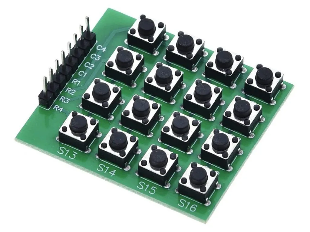
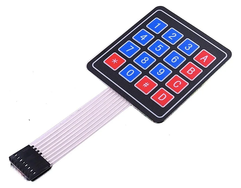
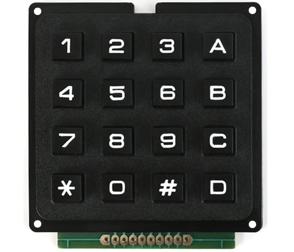
All the keypads in Figures 1-3 have the same schematics diagram (Figure 4).
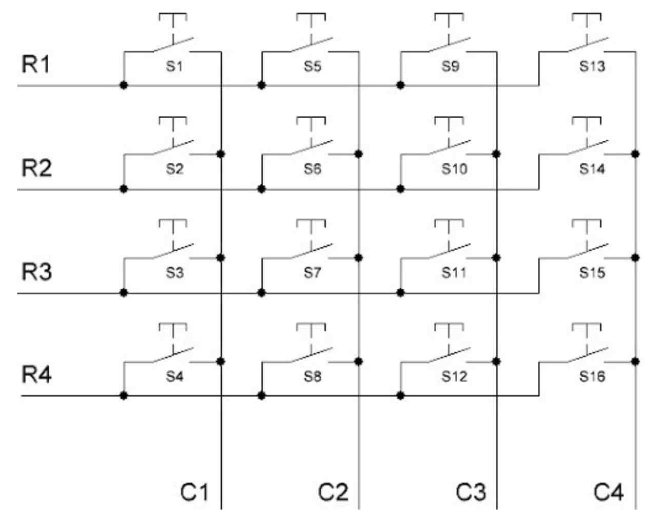
As you can see, the keypad consists of 16 pushbuttons S1 - S16. They are connected into a matrix 4x4, so each of four buttons in a row have one common pin (R1 - R4), and each of four buttons in a column also have one common pin (C1 - C4). Such a connection allows us to significantly reduce the number of the pins used for the keypad connection. Let’s compare the number of pins required for connecting the buttons separately and in matrix for different button numbers (Table 1).
Table 1 - Comparison of Pins Number for Separate Buttons and for Matrixes
| Number of Buttons | Matrix Size | Pin Numbers for Separate Connection | Pin Numbers for Matrix Connection |
| 1 | 1x1 | 1 | 2 |
| 4 | 2x2 | 4 | 4 |
| 12 | 3x4 | 12 | 7 |
| 16 | 4x4 | 16 | 8 |
| 25 | 5x5 | 25 | 10 |
| 60 | 6x10 | 60 | 16 |
| 100 | 10x10 | 100 | 20 |
As you can see, the matrix connection becomes much more beneficial with an increasing number of buttons. This is similar to the dynamic indication when you use the LED indicators.
But how do we operate with the matrix keypad? The algorithm is quite simple in fact:
- Configure all MCU pins to which columns are connected (C1 - C4) as outputs, and set them all high.
- Configure all MCU pins to which rows are connected (R1 - R4) as inputs with the pull-up resistors.
- Set one column pin low.
- Read all the row pins (R1 - R4). If no button in this row is pressed then all the readings will be “1” due to the pull-up resistors. If any button is pressed, then the corresponding reading will be “0” because initially we set the column pin low.
- Set the next column low and repeat step 4 for it.
- Repeat step 5 for all the columns.
In this way, you can distinguish what button was pressed. For example if we have pressed button S7 (fig. 4), we can find this out as we apply “0” to column C2 and read row R3. The same with all other buttons.
We will return to this algorithm when we consider the program code - for now let’s recall the math of music.
Notes Frequencies Calculation
Actually I have already described these calculations in the PIC10F200 series where I told how to play music using the PIC10F200 MCU. So I’ll just copy-paste this information here for your convenience.
As you most likely know, music is made of notes. There are seven basic notes - C, D, E, F, G, A, B (or H). Also, there are some “half-notes” which are located between some of the basic notes, they are called sharps or flats. So with the sharps (or flats) there are 12 “notes”: C, C#, D, D#, E, F, F#, G, G#, A, A#, B (or H).
Each note has its own frequency. As the foundation, we’ll use “A” of the 4’th octave and its frequency is 440 Hz. The frequencies of the neighboring notes can be calculated with the formula:

Yeah, music and mathematics are interconnected very tightly.
If you’ve ever seen a piano you might notice that there are more keys on it than 12. Yes, the notes are repeated. These 12 notes form an octave. And there can be several octaves on any musical instrument. The frequency of the same notes in the neighboring octaves differs by double. E.g. Note A at the fourth octave is 440 Hz, and note A one octave above is 880 Hz (Table 2).
Table 2 - Notes Frequencies
| Button | Note | F, Hz | Period, us | Half Period, 0.125us | CCPR1H | CCPR1L |
| S1 | C4 | 261.63 | 3822 | 15289 | 59 | 185 |
| S2 | C#4 | 277.18 | 3608 | 14431 | 56 | 95 |
| S3 | D4 | 293.66 | 3405 | 13621 | 53 | 53 |
| S4 | D#4 | 311.13 | 3214 | 12856 | 50 | 56 |
| S5 | E4 | 329.63 | 3034 | 12135 | 47 | 103 |
| S6 | F4 | 349.23 | 2863 | 11454 | 44 | 190 |
| S7 | F#4 | 369.99 | 2703 | 10811 | 42 | 59 |
| S8 | G4 | 392 | 2551 | 10204 | 39 | 220 |
| S9 | G#4 | 415.3 | 2408 | 9632 | 37 | 160 |
| S10 | A4 | 440 | 2273 | 9091 | 35 | 131 |
| S11 | A#4 | 466.16 | 2145 | 8581 | 33 | 133 |
| S12 | H4 (B4) | 493.88 | 2025 | 8099 | 31 | 163 |
| S13 | C5 | 523.25 | 1911 | 7645 | 29 | 221 |
| S14 | C#5 | 554.37 | 1804 | 7215 | 28 | 47 |
| S15 | D5 | 587.33 | 1703 | 6810 | 26 | 154 |
| S16 | D#5 | 622.25 | 1607 | 6428 | 25 | 28 |
In column “Button” there is a button from fig. 4 which will play the corresponding note from column “Note”. In column “F, Hz” there is a frequency of each used note in Hz, and in column “Period, us” there is a period that corresponds to this frequency, in microseconds. I will explain the last three columns later, when we consider the program code. For now just believe me, we need these values in our program.
But first, before proceeding to the program code, we need to consider the operation of the ECCP module in Compare mode.
Enhanced Capture/Compare/PWM (ECCP) Module
In tutorial 14 we already familiarized ourselves with the ECCP module, but that time we considered the Capture mode in detail.
As I already mentioned, in compare mode you can write some 16-bit value into the ECCP module register (CCPR1H and CCPR1L), and when the timer register reaches this value some events may happen, like: timer reset, pin change, interrupt generation, A/D conversion start. The event that will happen is configured by the CCP1M0-CCP1M3 bits of the CCP1CON register. We already considered them in tutorial 14 but let’s now look at the modes table one more time from the Capture mode perspective (Table 3).
Table 3 - ECCP Module Operation Modes Configuration
| CCP1M3 | CCP1M2 | CCP1M1 | CCP1M0 | Mode |
| 0 | 0 | 0 | 0 | Capture/Compare/PWM off (module reset) |
| 0 | 0 | 0 | 1 | Reserved |
| 0 | 0 | 1 | 0 | Compare mode, toggle output on match |
| 0 | 0 | 1 | 1 | Reserved |
| 0 | 1 | 0 | 0 | Capture mode, every falling edge |
| 0 | 1 | 0 | 1 | Capture mode, every rising edge |
| 0 | 1 | 1 | 0 | Capture mode, every 4th rising edge |
| 0 | 1 | 1 | 1 | Capture mode, every 16th rising edge |
| 1 | 0 | 0 | 0 | Compare mode, initialize CCP1 pin low, set output high on compare match (set CC1IPF bit) |
| 1 | 0 | 0 | 1 | Compare mode, initialize CCP1 pin high, set output low on compare match (set CC1IPF bit) |
| 1 | 0 | 1 | 0 | Compare mode, generate software interrupt only, CCP1 pin reverts the state |
| 1 | 0 | 1 | 1 | Compare mode, trigger special event (ECCP resets Timer1 or Timer3, start A/D conversion, set CC1IPF bit) |
| 1 | 1 | 0 | 0 | PWM mode: P1A, P1C active high; P1B, P1D active high |
| 1 | 1 | 0 | 1 | PWM mode: P1A, P1C active high; P1B, P1D active low |
| 1 | 1 | 1 | 0 | PWM mode: P1A, P1C active low; P1B, P1D active high |
| 1 | 1 | 1 | 1 | PWM mode: P1A, P1C active low; P1B, P1D active high |
In Table 3 I highlighted the Compare modes in green. Let’s consider them in detail.
When CCP1Mx bits are 0b0010, the ECCP module automatically toggles the output pin CCP1 (RC5) when the Timer1 register matches the ECCP register. I was considering using this mode in the current program but then decided to use another one.
When CCP1Mx bits are 0b1000 the ECCP module sets the CCP1 pin high when the Timer1 register matches the ECCP register.
When CCP1Mx bits are 0b1001 the ECCP module sets the CCP1 pin low when the Timer1 register matches the ECCP register.
When CCP1Mx bits are 0b1010 the ECCP module doesn’t affect the CCP1 pin state, it only triggers the interrupt.
When CCP1Mx bits are 0b1011 the ECCP module triggers the special event, which means that when the timer register matches the ECCP register, the timer registers resets, also A/D conversion can start if the ADC module is configured and enabled.
In all modes the match event triggers the interrupt and sets the CC1PF interrupt flag. which, as you should remember, must be cleared manually by the firmware.
In our program we will use the special event to reset the timer register at the compare event and thus set the required timer period as precisely as possible. This mode doesn’t affect the CCP1 pin, so will need to toggle the output pin manually.
Schematics Diagram
Let’s now consider the schematics diagram of the device (Figure 5).
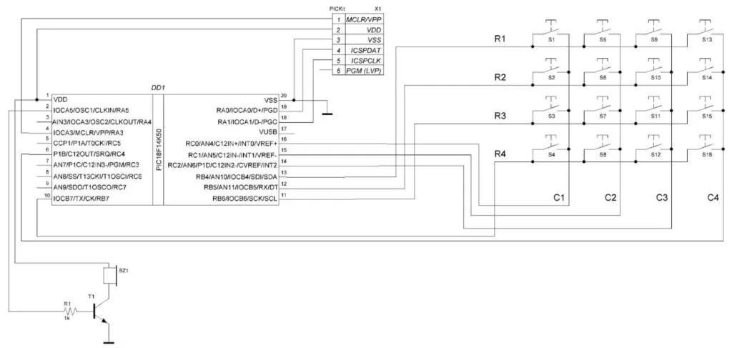
This schematic diagram consists of the PIC18F14K50 MCU (DD1), PICKit debugger (X1), 4x4 keypad (S1-S16), passive buzzer (BZ1), and the simple amplifier circuit based on transistor T1. The columns of the keypad (C1-C4) are connected to the RC0-RC3, and the rows of the keypad (R1-R4) are connected to pins RB4-RB7. These pins weren’t selected randomly. It’s more convenient if the columns and rows are connected to the consecutive pins of the same port, we will see why, when we consider the program code. Pins RB4-RB7 were selected because they have the internal pull-up resistors, unlike the pins of port C.
We will play the sound using the passive buzzer BZ1. I already explained in the doorbell tutorial of the previous series that passive buzzers can be piezoelectric or electromagnetic. The electromagnetic buzzer has the same construction as a regular speaker and has a low resistance, so to prevent the MCU pin from burning out, you need to add the amplification circuit. In our case it’s built with transistor T1 of the NPN structure, and resistor R1 of 1 kOhm that limits the transistor’s base current. The T1 transistor can be almost any type: I used BC547C, for instance, and it works quite well. If you have a piezoelectric buzzer, which has high input resistance, you can get rid of the R1 and T1 parts and connect the buzzer directly to the RA5 pin of the MCU.
Speaking of, as we will use the special trigger event of the ECCP module, which doesn’t directly affect the CCP1 pin, we can use any MCU pin to connect the buzzer, as we will toggle it manually. Thus I decided to use the RA5 pin, but actually you can use any available pin you want.
And that’s actually all about the schematic diagram, so let’s consider the programming code.
Program Code Description
#define _XTAL_FREQ 32000000 //CPU clock frequency


#include <xc.h>


uint16_t button;


void __interrupt() InterruptManager (void)	//Interrupt vector
{
     if(INTCONbits.PEIE == 1) //If peripheral interrupts are enabled
     {
    	if(PIE1bits.CCP1IE == 1 && PIR1bits.CCP1IF == 1) //If ECCP1 interrupt is enabled and ECCP1 interrupt flag is set
    	{
        	     PIR1bits.CCP1IF = 0; // Clear the ECCP1 interrupt flag
        	     LATAbits.LA5 ^= 1; //Toggle RA5 bit
    	}
     }
}


void main(void)
{
     //GPIO configure
     TRISB = 0xF0;       	//Configure RB port as inputs
     TRISC = 0xF0;       	//Configure RC0-RC3 pins as outputs
     TRISAbits.RA5 = 0;  	//Configure RA5 pin as output
     LATC = 0x0F;        	//Set RC0-RC3 pins high
     WPUB = 0xF0;        	//Enable pull-up resistors on port B
     INTCON2bits.NOT_RABPU = 0; //Enable pull-up resistors on ports A and B
     ANSELHbits.ANS10 = 0;   //Disable the analog buffers on RB4 pin
     ANSELHbits.ANS11 = 0;   //Disable the analog buffers on RB5 pin


//Oscillator module configuration
     OSCCONbits.IRCF = 6;	//Set CPU frequency as 8 MHz
     OSCTUNEbits.SPLLEN = 1; //Enable PLL


//Timer1 configuration
     T1CONbits.T1CKPS = 0;   //1:1 prescaler
     T1CONbits.T1OSCEN = 0;  //Disable Timer1 oscillator
     T1CONbits.TMR1CS = 0;   //Timer1 clock source is Fosc/4
     T1CONbits.TMR1ON = 1;   //Enable Timer1


//ECCP module configuration
     CCP1CONbits.CCP1M = 0b1011;//Compare mode, special event
     PIR1bits.CCP1IF = 0;	//Clear the ECCP interrupt flag
     T3CONbits.T3CCP1 = 0;   //ECCP module works with Timer1


//Interrupts configuration
     INTCONbits.GIE = 1; 	//Enable global interrupts
     INTCONbits.PEIE = 1;	//Enable peripheral interrupts


while (1)           	//Main loop of the program
     {
    	for (uint8_t i = 0; i < 4; i ++)//Loop for checking 4 rows
    	{
        	     LATC = ~(1 << i);//Set the corresponding row low
        	     __delay_ms (1); //Delay of 1 ms to let the voltage stabilize
        	     button = ((~PORTB & 0xF0) >> 4) << (i * 4); //Check the button row
        	     if (button) 	//If button value is not 0
        	     break;  	//Then leave from the loop
    	}
    	if (button)     	//If button value is not 0
    	{
        	     switch (button) //Check the button value
        	     {
            	          case 0x0001: CCPR1H = 59; CCPR1L = 185; break; //C4
            	          case 0x0002: CCPR1H = 56; CCPR1L = 95;  break; //C#4
            	          case 0x0004: CCPR1H = 53; CCPR1L = 53;  break; //D4
            	          case 0x0008: CCPR1H = 50; CCPR1L = 56;  break; //D#4
            	          case 0x0010: CCPR1H = 47; CCPR1L = 103; break; //E4
            	          case 0x0020: CCPR1H = 44; CCPR1L = 90;  break; //F4
            	          case 0x0040: CCPR1H = 42; CCPR1L = 59;  break; //F#4
            	          case 0x0080: CCPR1H = 39; CCPR1L = 220; break; //G4
            	          case 0x0100: CCPR1H = 37; CCPR1L = 160; break; //G#4
            	          case 0x0200: CCPR1H = 35; CCPR1L = 131; break; //A4
            	          case 0x0400: CCPR1H = 33; CCPR1L = 133; break; //A#4
            	          case 0x0800: CCPR1H = 31; CCPR1L = 163; break; //B4
            	          case 0x1000: CCPR1H = 29; CCPR1L = 221; break; //C5
            	          case 0x2000: CCPR1H = 28; CCPR1L = 47;  break; //C#5
            	          case 0x4000: CCPR1H = 26; CCPR1L = 154; break; //D5
            	          case 0x8000: CCPR1H = 25; CCPR1L = 28;  break; //D#5
        	     }
        	     PIE1bits.CCP1IE = 1;	//Enable the ECCP interrupts
    	}
    	else            	//If button value is 0
    	{
        	     LATAbits.LA5 = 0;   	//Set RA5 pin low
        	     PIE1bits.CCP1IE = 0;	//Disable the ECCP interrupts
    	}
     }
}
In line 1, we define the _XTAL_FREQ macro, this time as 32000000 because we need to have as high frequency as possible to achieve the best note generation accuracy.
In line 5 we declare the variable button of type uint16_t. This variable has 16 bits, each of which will represent the corresponding button state: “0” if the button is not pressed, and “1” if it is pressed.
In lines 7-17 there is the interrupt subroutine. It’s very similar to tutorial 14 because we use the same interrupt as there. So, in line 9, we check if the peripheral interrupts are enabled. In line 11, we check if the ECCP interrupt is enabled and if the ECCP interrupt flag is set (line 11). In this case we consider that the compare interrupt occurred because the Timer1 register (TMR1H and TMR1L) has matched the ECCP register (CCPR1H and CCPR1L). After that, we clear the interrupt flag (line 13), and toggle the RA5 pin (line 14). Actually this is the only payload of this subroutine - to toggle pin RA5, because the Timer1 register reset happens automatically regardless of the interrupt state at every compare event.
Actually, we could make another thing - toggle the CCP1 pin by the ECCP module (setting the CCP1Mx bits as 0b0010), and set the timer period the same way as in tutorial 8 by assigning the initial value for the timer register (I’ll leave this option for you as homework).
And this is all we do in the interrupt subroutine.
Now let’s consider the main function of the program (lines 19-89).
In line 22, we configure pins RB4-RB7 to which the row pins of the keypad are connected, as inputs (because 0xF0 corresponds to 0b11110000, so we set the four higher bits of the TRISB register as “1”). In line 23, we configure pins RC0-RC3 to which the column pins of the keypad are connected, as outputs, and in line 24, we configure pin RA5, to which the buzzer is connected, as output.
In line 25, we set pins RC0-RC3 high, according to the point 1 of the algorithm presented above. In line 26, we enable pull-up resistors on the RB4-RB7 pins, according to point 2 of the algorithm. Then, in line 27, we allow the pull-up resistors on ports A and B.
In lines 28 and 29 there is the register ANSELH which we didn’t consider before. Well, I think the time has come to start familiarizing you with the analog functions of the PIC18F14K50 MCU, even though we won’t use them for at least several tutorials. If you remember, in previous tutorials I avoided using the RB4 and RB5 pins as digital inputs, and said that this requires additional settings. If you look attentively at the MCU pins (fig. 5) you may notice that some pins have the letters AN with the following number from 3 to 11. These pins can operate as analog inputs, and by default they are configured in this mode. In this case the digital input buffer is disabled, so you can use these pins as digital outputs (as you could see in previous tutorials) but can’t use them as digital inputs, as the reading will always be 0. To enable the digital input buffer we need to disable the analog buffer. And to do this, there are two registers: ANSEL and ANSELH (ANalog SELect). If some bit of these registers is set to “1” then the digital input buffer is disabled, and if the bit is reset to “0” then the digital input buffer is enabled.
ANSEL has five active bits:
- bit #7 - ANS7 - enables/disables the digital buffer at RC3 pin;
- bit #6 - ANS6 - enables/disables the digital buffer at RC2 pin;
- bit #5 - ANS5 - enables/disables the digital buffer at RC1 pin;
- bit #4 - ANS4 - enables/disables the digital buffer at RC0 pin;
- bit #3 - ANS3 - enables/disables the digital buffer at RA4 pin.
ANSELH has four active bits:
- bit #3 - ANS11 - enables/disables the digital buffer at RB5 pin;
- bit #2 - ANS10 - enables/disables the digital buffer at RB4 pin;
- bit #1 - ANS9 - enables/disables the digital buffer at RC7 pin;
- bit #0 - ANS8 - enables/disables the digital buffer at RC6 pin.
So now you know how to use any pin as a digital input, and we will use this knowledge quite often in the future.
Now the sense of the lines 28-29 becomes clear - we enable the digital input buffers on pins RB5 (ANS11) and RB4 (ANS10).
In lines 32-33, we set the CPU frequency as 32 MHz by setting the internal oscillator to 8MHz (line 32) and enabling x4 PLL (line 33).
In lines 36-39, we configure Timer1: set the timer prescaler as 1:1 (line 36), disable Timer1 oscillator (line 37), set the Timer1 clock source as Fosc/4 (line 38), and finally enable Timer1 (line 39). Unlike the previous tutorial we don’t care about the 16-bit or 8-bit operation with the timer registers, as they will be updated by the ECCP module, so we don’t set or reset the RC16 bit.
In lines 42-44, we configure the ECCP module: set the compare mode, special trigger event (line 42), clear the interrupt flag (line 43), and assign the ECCP module to the Timer1 (line 44).
In line 47, we enable all unmasked interrupts, and in line 48 we enable the peripheral interrupts. And that’s all about the MCU initialization, so we can move to the main loop of the program (lines 50-88).
In lines 52-59 there is a loop to read the states of all buttons of the keypad. It works according to the algorithm that I wrote above. In line 52 we make the “for”-type loop from 0 to 4 to set all the columns low consequently and then read the rows.
In line 54 we set one of the pins of port C low. Let’s consider this line in more detail:
LATC = ~(1 << i);
So (1 << i) means “1” shifted by “i” positions to the left. The tilde means inversion of the result. Let’s see the values of the LATC register for all possible i values.
| i | (1 << i) | LATC = ~(1 << i) | Port C pin low |
| 0 | 0b00000001 | 0b11111110 | RC0 |
| 1 | 0b00000010 | 0b11111101 | RC1 |
| 2 | 0b00000100 | 0b11111011 | RC2 |
| 3 | 0b00001000 | 0b11110111 | RC3 |
I like such laconic yet powerful expressions that allow one to do a lot of things in several operations, and very soon you will see an even more tangled expression.
In line 55, we perform the delay of 1ms to let the voltage stabilize.
In line 56, there is one of the expressions that I like, which allows to read all the buttons states and save the result into one variable:
button = ((~PORTB & 0xF0) >> 4) << (i * 4);
As you remember, the rows of the keypad are connected to the RB4-RB7 pins, which correspond to the upper four bits of the PORTB register. Also the active pin level (when button is pressed) is low, so we need to invert the PORTB value if we want the “1” to represent the active value in the button variable. Then bitwise AND operation “&” between the inverted PORTB register and 0xF0 constant allows to reset the lower four bits of the result. Then we shift the result at four bits to the right. This is needed to shift the upper four bits to the position of the lower four bits. And finally we shift the obtained value to the left by the value (i * 4). This allows one to collect all the button values into one 16-bit variable. Let’s gather the interim and final result into table 4.
Table 4 - Results of the Button Calculation
| i | PORTB | ~PORTB | ~PORTB & 0xF0 | (~PORTB & 0xF0) >> 4) | ((~PORTB & 0xF0) >> 4) << (i * 4) | Active pin | Button |
| x | 11110000 | 00001111 | 00000000 | 00000000 | 0000000000000000 | No | No |
| 0 | 11100000 | 00011111 | 00010000 | 00000001 | 0000000000000001 | RB4 | S1 |
| 11010000 | 00101111 | 00100000 | 00000010 | 0000000000000010 | RB5 | S2 | |
| 10110000 | 01001111 | 01000000 | 00000100 | 0000000000000100 | RB6 | S3 | |
| 01110000 | 10001111 | 10000000 | 00001000 | 0000000000001000 | RB7 | S4 | |
| 1 | 11100000 | 00011111 | 00010000 | 00000001 | 0000000000010000 | RB4 | S5 |
| 11010000 | 00101111 | 00100000 | 00000010 | 0000000000100000 | RB5 | S6 | |
| 10110000 | 01001111 | 01000000 | 00000100 | 0000000001000000 | RB6 | S7 | |
| 01110000 | 10001111 | 10000000 | 00001000 | 0000000010000000 | RB7 | S8 | |
| 2 | 11100000 | 00011111 | 00010000 | 00000001 | 0000000100000000 | RB4 | S9 |
| 11010000 | 00101111 | 00100000 | 00000010 | 0000001000000000 | RB5 | S10 | |
| 10110000 | 01001111 | 01000000 | 00000100 | 0000010000000000 | RB6 | S11 | |
| 01110000 | 10001111 | 10000000 | 00001000 | 0000100000000000 | RB7 | S12 | |
| 3 | 11100000 | 00011111 | 00010000 | 00000001 | 0001000000000000 | RB4 | S13 |
| 11010000 | 00101111 | 00100000 | 00000010 | 0010000000000000 | RB5 | S14 | |
| 10110000 | 01001111 | 01000000 | 00000100 | 0100000000000000 | RB6 | S15 | |
| 01110000 | 10001111 | 10000000 | 00001000 | 1000000000000000 | RB7 | S16 |
Here you can see the metamorphoses of the bits that we are interested in (I marked them with yellow color). So, as you can see, after all, we have a strict correspondence between the position of “1” in the button variable and the pressed button.
In line 57, we check if the button value is not 0, which means that some button has been pressed. If so, we exit the loop immediately by calling the “break” command (line 58). This is needed to stop scanning the keypad in case we have detected that some button is pressed.
And actually this is all implementation of the keypad scanning algorithm. Now we can process the button variable. In line 60 we check if the button value is not 0. If so, we check what value has the button variable in the switch construction (lines 62 - 80). Let’s consider just one “case” line because others are the same, for example, line 64:
case 0x0001: CCPR1H = 59; CCPR1L = 185; break; //C4
The values at the “case” sentence (0x0001 and similar) correspond to the values from table 4, just in the hexadecimal system instead of binary (you can check this by yourself if you want). To understand why we assign these values to the CCPR1H and CCPR1L registers, we need to return to table 2.
Button S1 corresponds to note C4 which has the frequency 261.63 Hz, or a period of 3822.19 us. The main frequency of the CPU is 32 MHz, so the Timer1 input frequency is 32 / 4 = 8 MHz (because we didn’t use the timer prescaler). Thus, each tick of the timer is 1 / 8 = 0.125us. To reach the period of 3822 us we need 3822.19 / 0.125 = 30578 ticks of the timer. But during this period we need to toggle the output pin twice - first time from low to high in the middle of the period, and the second time from high to low at the end of the period, so we need to toggle the pin every 30578 / 2 = 15289 ticks. This is the value we have in the column “Half Period, 0.125us” of table 2. So in this column there is a number of timer ticks between the RA5 pin toggle.
Now, we need to split the value 15289 into two 8-bit numbers to load them to the CCPR1H and CCPR1L registers. To calculate the CCPR1H value we need to divide the 15289 by 256:
CCPR1H = 15289 / 256 = 59.
And CCPR1L is the modulo of division of 15289 by 256:
CCPR1L = 15289 - CCPR1H x 256 = 15289 - 59 x 256 = 185.
As you can see, these are exactly the same values that are in the first line of table 2.
In the same way the CCPR1H and CCPR1L values for other notes are calculated (lines 65 - 79).
Now, when we set the proper values of the ECCP registers, we need to enable the ECCP interrupt (line 81) to let the program toggle the RA5 pin inside the interrupt subroutine.
If the button value is 0 (line 83) we need to disable the ECCP interrupt (line 86) to stop RA5 toggling, and set the RA5 pin low (line 85) to remove power from the buzzer.
And that’s all about the program code. The device doesn’t need any adjustment and, being assembled correctly, starts working at once.
As for homework, I already have formulated it earlier, but let me copy it here for your convenience: make the same task but toggle the CCP1 pin by the ECCP module (set the CCP1Mx bits as 0b0010), and set the timer period the same as in tutorial 8 by assigning the initial value for the timer register inside the Timer1 overflow interrupt.

Get the latest tools and tutorials, fresh from the toaster.


