An Overview of Controlling Temperature with PID | Embedded C Programming - Part 20
Published
Hello! This tutorial will be very big and complex and contain large amounts of both theoretical and practical work. Also the code size will be the biggest among other tutorials we considered before.
As follows from the title of this tutorial, this time we will create a temperature PID controller. On circuitbread.com there is a series of articles devoted to the theory of automated control. These tutorials are very good but in my opinion (and not only in mine) their only flaw is that they are all theoretical (thus far). For sure, there are simulations of the control systems in SciLab but still it’s not the same as if you hold a real device in your hands. So I was asked by Josh to write the tutorial in which I will merge the two topics: microcontroller programming and automated control theory. As I’m a bit familiar with both of them from my time as a University teacher, I agreed with pleasure. And thus you are now able to enjoy (I hope) the results of my modest work.
This tutorial will be split into three parts: the first one will be devoted to the hardware and the theoretical background, the second to the programming code, and the third to the practical experiments. So, let’s start!
PID Control System Description
First of all, I want to mention that I expect from you some knowledge of automated control theory which you can find in the circuitbread.com or other resources. Because this tutorial is not about the basics of automated control but about its practical application, you need to have at least some minimal background.
General schematics diagram of the PID control system was considered in the tutorial Proportional, Integral, and Derivative Control 4.2. Let’s repeat it here (Figure 1).
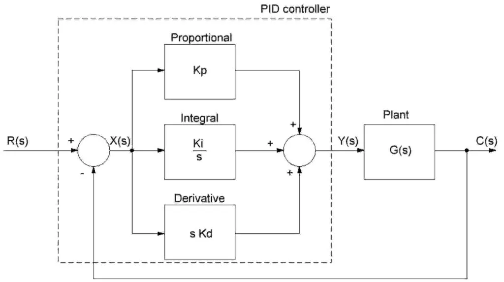
As you can see, the whole system consists of two main parts: the PID controller which has some internal parts, and the plant with the transfer function G(s). In our case the whole PID controller part will be implemented utilizing a PIC18F14K50 MCU, and the plant will be separate.
As follows from the tutorial title, we will control the temperature of the plant. I was thinking about what to use as a heater because the thing should be widespread, simple and safe so as not to burn down the house. Finally my choice fell on a 5W resistor with the resistance of 10-15 Ohm (Figure 2).

As you can see, this resistor is rectangular unlike less powerful ones, so it’s simpler to attach the temperature sensor to its surface to have better thermal contact. As a sensor which will be needed to measure the temperature of the resistor we will use the familiar from the tutorial 12 DS18B20. This sensor will produce the output signal of the system C(s) which represents the current value of the resistor’s temperature (see Figure 1).
The R(s) signal is the input value of the system which represents the temperature setpoint. This value will be set by the incremental encoder. I recommend using the encoder module from an Arduino set (Figure 3).
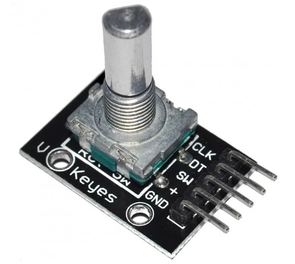
We will consider its operation later, and now let’s return to Figure 1 and look into the system equation in more detail.
PID Control Algorithm Implementation on the MCU
The input and output signals of the system are applied to the input of the PID controller, where they are compared in a summing device. At the output of this device we obtain the error signal X(s):

This signal is applied to the three control blocks: proportional, integral, and derivative, the output of which are summed in another summing device and form the control impact Y(s):

Here Kp, Ki and Kd are proportional, integral, and derivative factors of the regulator which we need to find to let it work properly. The signal Y(s) is applied to the input of the plant and changes its output to minimize the error signal X(s).
Both summing devices and three control blocks are implemented in program code of the MCU. So our task is to convert the equations (1) and (2) to the normal view which can be processed by the MCU. To do this, let’s switch from the Laplace form of the equations to the time-based ones:


To get rid of the integral let’s differentiate both part of the equation (4):

Still doesn’t look like an equation that can be calculated with the MCU. Now we need to make one more transformation which will make everything clear both for us and the CPU. We need to remember that the derivative of the function is the limit of the ratio between the function increment and the argument increment when the last nears 0:

But what if we don’t aim the Δx to 0 but set it as some small but non-zero value which we will call step “h”, now we can rewrite the equation 6 as follows:

Let’s now rewrite the equation (5) considering the equation (7):

As you see the last member still consists of the the derivative which we need to make discrete or discretize:


Let’s now multiply both parts of the equation by “h”:

And finally:

This is the equation we can use in the program. To calculate the control impact at the current moment Y(t) we need to know the control impact at the previous step Y(t-h), and the error signal at the current moment X(t), at the previous step X(t-h) and two steps ago X(t-2h). The smaller the time step h is, the better the calculation accuracy. At the beginning, we don’t have the values at the previous steps, so we assign these values as 0.
As you see, the whole PID control algorithm can be implemented on just one line of the code and can be used even on small and weak MCUs. There are certain problems though which we will consider in the second part of the tutorial.
I think now we know enough to formulate the whole task of this big tutorial:
- Create the temperature control system, in which the plant is the 5W resistor, the sensor is a DS18B20, and the PID control is implemented inside the PIC18F14K50 MCU.
- The setpoint should be set by the incremental encoder.
- All the system parameters (setpoint, current temperature, control impact, current time) should be displayed on the 1602 LCD.
- The system should work in two modes: manual, in which we set the control impact [Y(s)] by rotating the encoder handle; and automated, in which we set the setpoint of the temperature, and the control impact is calculated by the PID algorithm.
Schematics Diagram of the System
As we have the task clear now, let’s proceed to the schematics diagram of the system (Figure 4).
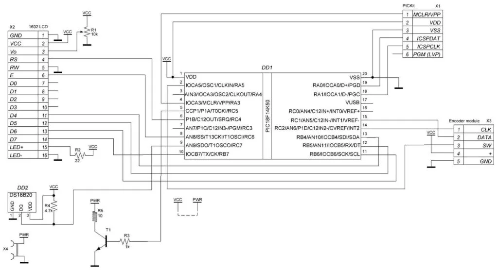
We’ve already dealt with almost all parts in Figure 4. DD1 is PIC18F14K50 MCU, X1 is the PICKit debugger. X2 is the 1602 LCD which we considered in tutorial 18. Please note that the connection of the LCD differs from the previous time. This was done because we need some pins of the port C for other purposes. Now we connected the data pins D4-D7 of the LCD to the pins RB4-RB7 of the MCU, RS pin remains connected to the RC4 pin of the MCU, and the E pin is connected to the RC6 pin instead of RC5 because the RC5 pin is used by the PWM module (see tutorial 14). Resistor R1 sets the contrast of the LCD, and resistor R2 limits the current through the backlight LED of the LCD.
The DS18B20 sensor (DD2) is connected to pin RC7 unlike tutorial 12 where we met it the first time. Resistor R4 is the pull-up which is required for proper operation of the sensor.
Resistor R5 is the 10 Ohm, 5 W, and acts like a plant of the control system. As it will dissipate a lot of power and consume a lot of current, we need to use the key transistor T1. Please pay attention that the upper pin of the resistor R5 is connected to the PWR net, not to VCC from which the rest of the circuit is powered. This is needed for the same reason - high current through the resistor R5. If we power the device from the PICKit programmer, it will be unable to provide the necessary power and either will not run at all or will be damaged. So we need to apply external power through the connector X4. I recommend using a USB connector and 5V power source either from the USB port of the PC or laptop or from the mobile phone charger. With this voltage and the 10 Ohm resistor the current will be I = 5V / 10Ohm = 0.5A, which is normal according to USB specification. And the maximum power will be P = 5V x 0.5A = 2.5W. So the resistor will not burn. Also I recommend you use the transistor T1 with a low value of the emitter-collector voltage drop and the collector current more than 600mA. I used the Darlington NPN transistor BDW93. Resistor R4 limits the base current of transistor T1.
If you want, you can merge the PWR and VCC sources as shown in Figure 4 with the dash line. In this case you don’t need to power the device from the PICKit and don’t select this option in the PICKit settings.
By the way I’ve found a very interesting thing on the Thingiverse.com site which allows one to power directly from a USB port using typical male Dupont cables (Figure 5).
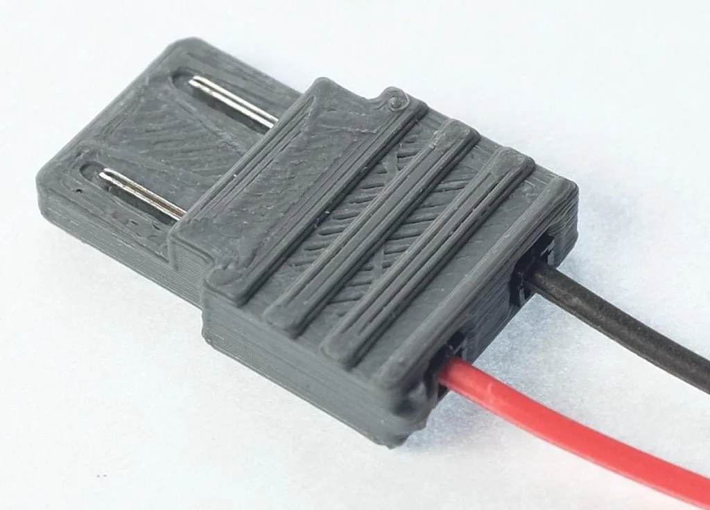
I’ve printed a couple of such adapters and so far I am very satisfied with them.
And the last thing is the encoder module X3 shown in Figure 3. Let’s consider it in more detail. Usually the encoder has two (or, more rarely, three) outputs called A, B (and Z). When you rotate the handle of the encoder, outputs are connected to the common pin with a certain consequence. Let’s consider it for the 2-outputs encoder (Figure 6).
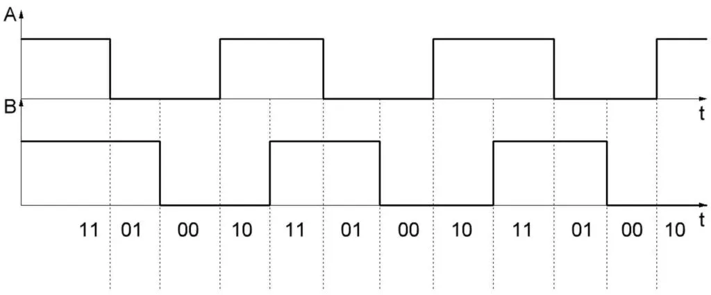
As you can see, during rotating the encoder’s shaft the signals A and B change their state with some shift. This shift allows us to distinguish the direction of rotation of the encoder. So for example if the current state is “11” which means that both A and B pins are high, then if the next state is “01” then the rotation is clockwise, and if the next state is “10” then the rotation is counterclockwise.
In the encoder module presented in Figure 3 when you rotate the shaft, you can feel some clicks. Each click corresponds to four consequent changes of the encoder state from “11” to “11” state either as “11”-”01”-”00”-”10”-”11” or as “11”-”10”-”00”-”01”-”11”. As you see, the sequences are different so even in this case you can detect the rotation direction. You just need to remember that there are four state changes per one click, not one.
Also if you look at the code sequences you can notice that the neighboring states differ only by one bit. Such a sequence is called Gray code. This code is often used in absolute encoders (which we will not consider here) because it’s easier to make the coding disks in it. We won’t need it, this is just an FYI - we will use the Gray code in our program and convert it into regular binary code to calculate the encoder steps, but let’s leave this for the next part of the tutorial, and now let’s return to schematics diagram (Figure 4).
As you can see, the encoder module has five pins, and none of them are called A or B. I actually don’t know why, but for some reason these pins are called “DATA” and “CLK” correspondingly. Maybe there is a reason for this, but for me it’s just confusing.
So we connect these “DATA” and “CLK” pins of the encoder to the RC1 and RC2 pins of the MCU correspondingly. The choice of the MCU pins is not random, the RC1 and RC2 pins are merged with the external interrupts INT1 and INT2 about which we will talk a bit later.
The “SW” pin of the encoder stands for the “switch”. If you press on the encoder handle, you can also feel the click. This is the usual switch which is merged with the encoder shaft, which we will use in our system to toggle between the manual and automated modes. We connect this pin to the RA5 pin of the MCU. Actually, we can connect it to any pin with the internal pull-up resistor. As all pins of port B are already busy, I used the first free pin of port A.
The “+” pin should be connected to VCC. Inside the module there are pull-up resistors connected to “DATA” and “CLK” pins, so you can connect these pins even to those MCU pins which don’t have the internal pull-up resistors. There is also a spot for the resistor connected to the switch but for some reason in my module it’s not placed. If you use internal pull-up resistors for all encoder pins, you can leave the “+” pin unconnected.
The “GND” pin’s name speaks for itself. This is the common pin of the encoder, and it should be connected to ground.
And I think that’s all about the schematics diagram. Let’s now consider new MCU modules that we will need to use in our program.
External Interrupts INTn
As follows from their name, external interrupts cause an interrupt when some external event happens, which in this case is change of the state of the dedicated pin. There are three pins, each of which can cause the interrupt: INT0 (merged with RC0), INT1 (merged with RC1), and INT2 (merged with RC2).
The interrupt may happen either on the rising or on the falling edge of these pins. The edge is selected by special bits which we will consider very soon. Also these interrupts have a feature to wake the CPU from the sleep mode, which can be useful in low-power applications.
These interrupts don’t belong to the peripherals, so to enable them you only need to enable the GIE bit, and don’t need to enable the PEIE bit (this is separate from the individual interrupts masking bits).
Let’s consider the registers which configure the INTn interrupts:
INTCON register which we already meet in tutorials 8:
- bit #7 - GIE/GIEH (Global Interrupt Enable bit). It has two meanings depending on the value of the IPEN bit.
- If IPEN = 0: Setting this bit to 1 enables all unmasked interrupts, resetting it to 0 disables all interrupts including peripherals.
- If IPEN = 1: Setting this bit to 1 enables all high-priority interrupts, resetting it to 0 disables all interrupts including low priority.
- bit #6 - PEIE/GIEL (Peripheral Interrupt Enable bit). It also has two meanings depending on the value of the IPEN bit.
- If IPEN = 0: Setting this bit to 1 enables all unmasked peripheral interrupts, resetting it to 0 disables all peripheral interrupts.
- If IPEN = 1: Settings this bit to 1 enables all low-priority interrupts, resetting it to 0 disables all low priority interrupts.
- bit #4 - INT0IE (INT0 External interrupt enable). Setting this bit to 1 enables the INT0 interrupt, resetting this bit to 0 disables the INT0 interrupt.
- bit #1 - INT0IF (INT0 External Interrupt Flag bit). This bit is set to 1 by hardware. If it’s set to 1 then the INT0 interrupt has occurred, if it’s 0 then no INT0 interrupt occurred. When set, this bit should be cleared by software.
INTCON2 register which we also already met in tutorial 4:
- bit #6 - INTEDG0 (INT0 External interrupt edge select). If this bit is 0 then the interrupt can occur on the falling edge, and if this bit is 1 then the interrupt can occur on the rising edge.
- bit #5 - INTEDG1 (INT1 External interrupt edge select). If this bit is 0 then the interrupt can occur on the falling edge, and if this bit is 1 then the interrupt can occur on the rising edge.
- bit #4 - INTEDG2 (INT2 External interrupt edge select). If this bit is 0 then the interrupt can occur on the falling edge, and if this bit is 1 then the interrupt can occur on the rising edge.
- bit #2 - TMR0IP (Timer0 overflow interrupt priority). If this bit is 0 then this interrupt has low priority, and if it is 1 then the interrupt has high priority.
INTCON3 register is totally devoted to INTn interrupts:
- bit #7 - INT2IP (INT2 external interrupt priority). If this bit is 0 then this interrupt has low priority, and if it is 1 then the interrupt has high priority.
- bit #6 - INT1IP (INT1 external interrupt priority). If this bit is 0 then this interrupt has low priority, and if it is 1 then the interrupt has high priority.
- bit #4 - INT2IE (INT2 External interrupt enable). Setting this bit to 1 enables the INT2 interrupt, resetting this bit to 0 disables the INT2 interrupt.
- bit #3 - INT1IE (INT1 External interrupt enable). Setting this bit to 1 enables the INT1 interrupt, resetting this bit to 0 disables the INT1 interrupt.
- bit #1 - INT2IF (INT2 External Interrupt Flag bit). This bit is set to 1 by hardware. If it’s set to 1 then the INT2 interrupt has occurred, if it’s 0 then no INT2 interrupt occurred. When set, this bit should be cleared by software.
- bit #0 - INT1IF (INT1 External Interrupt Flag bit). This bit is set to 1 by hardware. If it’s set to 1 then the INT1 interrupt has occurred, if it’s 0 then no INT1 interrupt occurred. When set, this bit should be cleared by software.
Please note, that INT0 interrupt doesn’t have the interrupt priority bit. This is because INT0 always has a high priority.
And that’s everything about these interrupts. You just need to remember that even if you configure the interrupts here, you still need to configure your pin as an input to make it work properly.
Timer2 Module
We already are familiar with Timer0 and Timer1, so it’s time to get acquainted with Timer2. This timer is very much different from the ones that we already considered. So let’s see what are its main features:
- 8-bit timer (TMR2) and period (PR2) registers;
- Readable and writable both registers;
- Software programmable prescaler and postscaler (from 1:1 to 1:16 each);
- Interrupt on TMR2-on-PR2 match.
So unlike other timers, this one only works in 8-bit mode, so it can only count up to 0xFF (or 255). Also it has two registers: timer register TMR2 and period register PR2. The interrupt happens not on the overflow of the TMR2 register but on a match of the TMR2 and PR2 registers. Also when the match happens, the TMR2 register resets to 0. So it’s easier to set the precise frequency of Timer2 by just setting the right value of the PR2 register. The default value of PR2 after reset is 0xFF.
Also, unlike other timers, this one has both a prescaler and postscaler. Prescaler divides the input frequency of the timer, while postscaler divides the output frequency of the timer. The postscaler can be used for generating the interrupts more rarely, but when Timer2 is used for generating the PWM signal, the postscaler is not applicable.
To configure the Timer2 there is the register T2CON:
- bits #6-#3 - T2OUTPS<3:0> (Timer2 output postscaler):
T2OUTPS3 | T2OUTPS2 | T2OUTPS1 | T2OUTPS0 | Postscaler |
0 | 0 | 0 | 0 | 1:1 |
0 | 0 | 0 | 1 | 1:2 |
0 | 0 | 1 | 0 | 1:3 |
0 | 0 | 1 | 1 | 1:4 |
0 | 1 | 0 | 0 | 1:5 |
0 | 1 | 0 | 1 | 1:6 |
0 | 1 | 1 | 0 | 1:7 |
0 | 1 | 1 | 1 | 1:8 |
1 | 0 | 0 | 0 | 1:9 |
1 | 0 | 0 | 1 | 1:10 |
1 | 0 | 1 | 0 | 1:11 |
1 | 0 | 1 | 1 | 1:12 |
1 | 1 | 0 | 0 | 1:13 |
1 | 1 | 0 | 1 | 1:14 |
1 | 1 | 1 | 0 | 1:15 |
1 | 1 | 1 | 1 | 1:16 |
- bit #2 - TMR2ON (Timer2 on). When this bit is 0 then Timer2 is off, when it is 1 then Timer2 is on.
- bits #1-#0 - T2CKPS<1:0> (Timer2 Clock prescaler):
T2CKPS1 | T2CKPS0 | Prescaler |
0 | 0 | 1 |
0 | 1 | 4 |
1 | 0 | 16 |
1 | 1 | 16 |
As you can see, almost all bits of the T2CON register set either prescaler or postscaler value.
To control the Timer2 interrupts, we use the registers PIE1 and PIR1 which we already met in tutorial 14 when considering Timer1. For Timer2 the bits even have almost the same names: TMR2IE (bit #1) in register PIE1 to enable Timer2 TMR2-to-PR2 match interrupt, and TMR2IF (bit #1) in register PIR1 as the interrupt flag. This interrupt belongs to the peripheral ones, so you need to enable both GIE and PEIE bits to allow them.
And that’s everything about Timer2, it is, in fact, quite primitive.
ECCP Module in PWM Mode
We have considered the ECCP module in tutorial 14 (Capture mode) and in tutorial 16 (Compare mode). Now, there is only one mode that we didn’t use before, namely PWM.
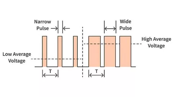
As you know, PWM stands for Pulse Width Modulation, which means that we can change the duty cycle of the pulses on some pin to change the average voltage on it. This method is very widespread and became a de-facto standard in motor control, DC-DC converters, heaters, dimming lights and other devices where the voltage regulation is required. If you read the PIC10F200 series, you can remember that we used it there as well. But that time we generated it by the program code (bit-banging), and now we will use the special dedicated hardware module for this.
Let’s first look one more time at the bits CCP1M0-CCP1M3 of the register CCP1CON that configure the mode of the module (table 1), which we already saw in tutorial 14 and tutorial 16.
Table 1 - ECCP module operation modes configuration
CCP1M3 | CCP1M2 | CCP1M1 | CCP1M0 | Mode |
0 | 0 | 0 | 0 | Capture/Compare/PWM off (module reset) |
0 | 0 | 0 | 1 | Reserved |
0 | 0 | 1 | 0 | Compare mode, toggle output on match |
0 | 0 | 1 | 1 | Reserved |
0 | 1 | 0 | 0 | Capture mode, every falling edge |
0 | 1 | 0 | 1 | Capture mode, every rising edge |
0 | 1 | 1 | 0 | Capture mode, every 4th rising edge |
0 | 1 | 1 | 1 | Capture mode, every 16th rising edge |
1 | 0 | 0 | 0 | Compare mode, initialize CCP1 pin low, set output high on compare match (set CC1IPF bit) |
1 | 0 | 0 | 1 | Compare mode, initialize CCP1 pin high, set output low on compare match (set CC1IPF bit) |
1 | 0 | 1 | 0 | Compare mode, generate software interrupt only, CCP1 pin reverts the state |
1 | 0 | 1 | 1 | Compare mode, trigger special event (ECCP resets Timer1 or Timer3, start A/D conversion, set CC1IPF bit) |
1 | 1 | 0 | 0 | PWM mode: P1A, P1C active high; P1B, P1D active high |
1 | 1 | 0 | 1 | PWM mode: P1A, P1C active high; P1B, P1D active low |
1 | 1 | 1 | 0 | PWM mode: P1A, P1C active low; P1B, P1D active high |
1 | 1 | 1 | 1 | PWM mode: P1A, P1C active low; P1B, P1D active high |
I highlighted the PWM modes with the blue color. As you can see there are not that many of them. But don’t worry, there are other bits in this register that expand the mode number significantly. But first let’s look at table 1.
As follows from the highlighted lines, PWM can be generated at up to four outputs: P1A (RC5), P1B (RC4), P1C (RC3), P1D (RC2). Active high means that the pulses are positive, and active low means that the pulses are negative. The first option is selected when the NPN or N-channel FETs are used, and the second option is selected when the PNP or P-channel FETs are used as key transistors to control the load. In our case we use the NPN transistor, so we need to select the active high option. As we will generate the PWM pulses at the P1A (RC5) pin (see Figure 4) we need to set the CCP1Mx bits either as 0b1100 or as 0b1101.
Let’s now consider the other bits of the CCP1CON register, as they are related to the PWM mode as well:
- bits #7-#6 - P1M <1:0> (Enhanced PWM output configuration):
P1M1 | P1M0 | Output configuration |
0 | 0 | Single output. P1A, P1B, P1C, and P1D are controlled by steering (see about it below) |
0 | 1 | Full-bridge output forward: P1D modulated, P1A active, P1B and P1C inactive |
1 | 0 | Half-bridge output: P1A and P1B modulated with dead-band control; P1C and P1D not used by the module |
1 | 1 | Full-bridge output reverse: P1B modulated, P1C active, P1A and P1D inactive |
- The full-bridge and half-bridge configurations are mainly used in motor control applications, so we will not consider them here in detail, maybe I will make a separate tutorial about this later.
- bits #5-#4 - DC1B <1:0> (PWM duty cycle bit 1 and bit 0). And here is a very weird and confusing thing to me. The ECCP module is claimed to be “enhanced”, and it really has a lot of modes and options. But for some reason, for PWM generation, it uses Timer2 which is only 8 bits, so the maximum expected PWM resolution is just 256 steps. But they expanded the resolution by 2 bits in a tricky way, so the real maximum PWM resolution is 10 bits, or 1024 steps.
And one more weird thing. The upper 8 bits of the PWM register are located in the CCPR1L register, and the lower 2 bits are DC1B1 and DC1B0. I don’t know why they don’t use the lower two bits of CCPR1H register as the upper two PWM bits, and the CCPR1L register as lower eight PWM bits, which would be clear and logical. But we have what we have (I don’t remember how many times I used this phrase in this current series).
As for increasing the resolution of Timer2, this is even more weird. As follows from the PIC18F14K50 data sheet, “The 8-bit timer TMR2 register is concatenated with the 2-bit internal Q clock, or 2 bits of the prescaler to create the 10-bit time base”. And that’s all the available information about this subject. As I understand, Timer2 is clocked with the Fosc/4 frequency. But, in fact, the MCU main frequency is Fosc. It is divided by 4 because it takes 4 ticks to implement every command, and to count up to 4 we need exactly 2 bits, that’s how we get the missing 2 bits of the Timer2 resolution. As for the part about the prescaler, I guess that if the prescaler is not 1:1 then the timer is clocked with a lower frequency than Fosc/4, and to get the 10-bit resolution, the prescaler’s bits are counted in as well. That’s an odd and complex yet interesting solution.
There are several registers to control the ECCP module in PWM mode, but I will not consider them in detail now, just enumerate and give a brief description:
- ECCP1AS - ECCP auto-shutdown control register;
- PWM1CON - Enhanced PWM control register;
- PSTRCON - Pulse steering control register. Let’s consider this one in detail, as an exception, as we will use it in our program:
- bit #3 - STRD (Steering enable bit D). If this bit is 1 then the P1D pin has the PWM waveform with polarity control from CCP1Mx bits. If this bit is 0 then P1D operates as usual GPIO (RC2).
- bit #2 - STRC (Steering enable bit C). If this bit is 1 then the P1C pin has the PWM waveform with polarity control from CCP1Mx bits. If this bit is 0 then P1C operates as usual GPIO (RC3).
- bit #1 - STRB (Steering enable bit B). If this bit is 1 then the P1B pin has the PWM waveform with polarity control from CCP1Mx bits. If this bit is 0 then P1B operates as usual GPIO (RC4).
- bit #0 - STRA (Steering enable bit A). If this bit is 1 then the P1A pin has the PWM waveform with polarity control from CCP1Mx bits. If this bit is 0 then P1A operates as usual GPIO (RC5).
So by setting the bits STRx you can select which pins will generate the PWM signal, which is quite convenient. Also you shouldn’t forget to configure the used pins as outputs by resetting the corresponding bits of the TRISC register. Also, I should mention that the PWM steering works only in single-output PWM mode (P1M1 = 0 and P1M0 = 0, CCP1M3 = 1 and CCP1M2 = 1).
And that’s finally the last of the theoretical portion of this tutorial. In the next part we will consider the programming code. I will make two versions of if: without using MCC, and with it.

Get the latest tools and tutorials, fresh from the toaster.


