How to use the PWM Function of Timer Array Unit (TAU) | Renesas RL78 - 10
Published
Hi! Welcome back to CircuitBread. In the previous tutorial, we discussed the internal ADC of the RL78 MCU. This time, we will try using the ADC function together with the PWM function of the RL78 Timer Array Unit (TAU). We will not discuss what PWM is and its applications anymore. You can read this EEFAQ: What is a PWM signal? or watch this video: How do PWMs work? In this tutorial, we will only discuss how the PWM function of the RL78 TAU works and then provide an example where we vary the duty cycle of the PWM output signal using the analog value read across the analog input channel of the RL78 ADC.
Registers Controlling TAU PWM Function
Timer Array Unit Registers | Bit/s and Register/s used in the Sample Project |
|---|---|
Peripheral Enable Register 0 (PER0) | TAU1EN Bit |
Timer Clock Select Register m (TPSm) | TPS1 Register |
Timer Mode Register mn (TMRmn) | TMR10 & TMR11 Registers |
Timer Channel Enable Status Register m (TEm) | TE1 Register |
Timer Channel Stop Register m (TTm) | TT1 Register |
Timer Channel Start Register m (TSm) | TS1 Register |
Timer Output Enable Register m (TOEm) | TOE1 Register |
Timer Output Register m (TOm) | TO1 Register |
Timer Output Level Register m (TOLm) | TOL1 Register |
Timer Output Mode Register m (TOMm) | TOM1 Register |
Timer Count Register mn (TCRmn) | TCR10 & TCR11 Registers |
Timer Data Register mn (TDRmn) | TDR10 & TDR11 Registers |
Port Register (Pxx) | P6 Register |
Port Mode Register (PMxx) | PM6 Register |
TAU Channel 10 Count End/Capture End (INTTM10) Interrupt Mask Flag | TMMK10 Bit |
TAU Channel 10 Count End/Capture End (INTTM10) Interrupt Request Flag | TMIF10 Bit |
TAU Channel 11 Count End/Capture End (INTTM11) Interrupt Mask Flag | TMMK11 Bit |
TAU Channel 11 Count End/Capture End (INTTM11) Interrupt Request Flag | TMIF11 Bit |
TAU Channel 10 Count End/Capture End (INTTM10) Priority Specification Flags | (TMPR110, TMPR010) Bits |
TAU Channel 11 Count End/Capture End (INTTM11) Priority Specification Flags | (TMPR111, TMPR011) Bits |
Table 1. Registers Controlling RL78 TAU PWM Function.
The table above shows the bits and registers used to control the PWM function of the TAU. Except for the Timer Output Level Register m (TOLm) and the Timer Output Mode Register m (TOMm), these bits and registers were already discussed in the previous tutorials: Renesas RL78 - 7. microsecond Delay Function using the Timer Array Unit (TAU), Renesas RL78 - 4. General Purpose Input/Outputs (GPIOs), Renesas RL78 - 5. Interrupt Functions. So we don’t need to discuss them in detail anymore. Please review the previous tutorials.
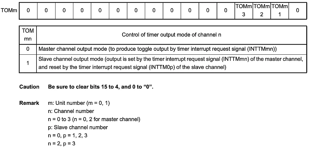
Regarding the TOLm and TOMm registers, the TOLm register is used to set each channel’s timer output level (positive or negative logic), while the TOMm register is used to set the timer output mode (master or slave channel output mode). A 16-bit memory manipulation instruction can set both registers.. The images below show the settings of the TOLm and the TOMm registers.


RL78 TAU PWM Function Operation
As shown in the image below, the TAU of the RL78 MCU supports the PWM function by utilizing two channels, one master and one slave channel. The master channel operates in interval timer mode, while the slave operates in one-count mode. The operation clock can be CKm0 or CKm1. However, the master and slave channels should use the same operation clock.
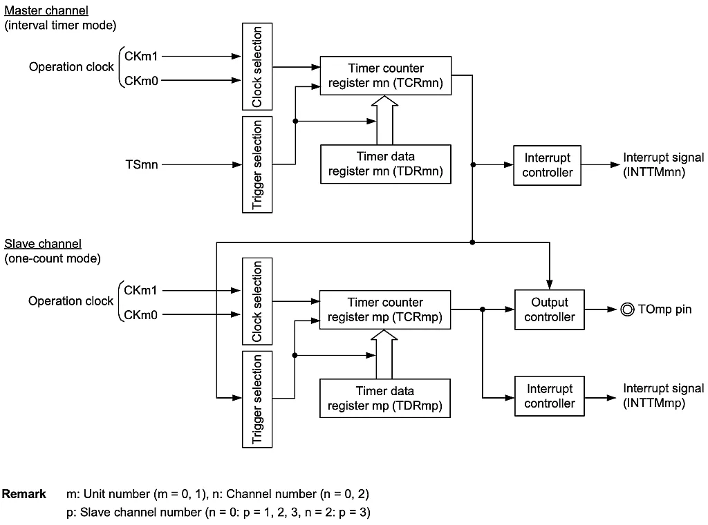
The operation of the TAU PWM function starts by setting the master channel start trigger bit (TSmn) to 1. In this case, the master channel interrupt (INTTMmn) is generated (make sure the MDmn0 bit of the TMRmn register is set to 1 so that INTTMmn is generated when counting is started), the value in the master channel TDR register (TDRmn) is loaded to the master channel TCR register (TCRmn), and the counter starts counting down.
The interrupt INTTMmn generated by the master channel serves as the start trigger of the slave channel. So when INTTMmn is generated after setting the TSmn bit, the value in the slave channel TDR register (TDRmp) is loaded in the slave channel TCR register (TCRmp), and the counter of the slave channel starts counting down too.
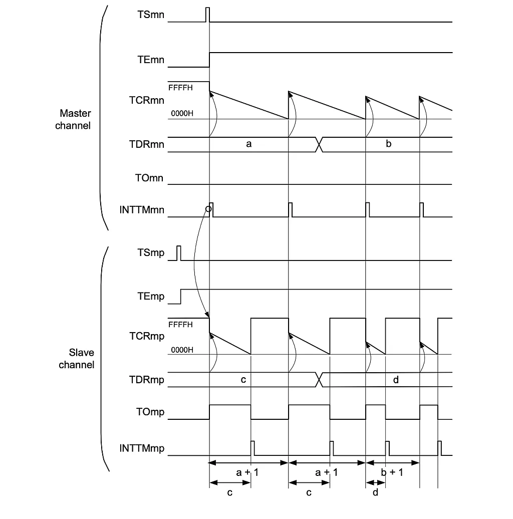

When the counter of the master channel reaches 0000H, the INTTMmn interrupt is generated, the value of the TDRmn register is loaded again to the TCRmn register, and the master channel counter counts down again. This operation is repeated until the channel stop trigger bit (TTmn) of timer channel stop register m (TTm) is set to 1.
In the slave channel case, when its counter reaches 0000H, the slave channel interrupt (INTTMmp) is generated, and the slave channel waits until the next start trigger (INTTMmn from the master channel) is generated for its counter to count down again.

The period of the PWM signal is the time until the master channel counts down to 0000H while the duty cycle depends on the time until the slave channel counts down to 0000H. The PWM output across the TOmp pin goes HIGH one clock after the master channel generates INTTMmn and goes LOW when the TCRmp register of the slave channel becomes 0000H. Figure 5 shows how you can calculate the period and the duty cycle of the PWM signal. When the TDRmp value is 0, the duty cycle is 0%. If the value is equal to or greater than [TDRmn value + 1], the duty cycle is 100%.
A reminder from the hardware user’s manual:
“To rewrite both timer data register mn (TDRmn) of the master channel and the TDRmp register of the slave channel, a write access is necessary two times. The timing at which the values of the TDRmn and TDRmp registers are loaded to the TCRmn and TCRmp registers is upon occurrence of INTTMmn of the master channel. Thus, when rewriting is performed split before and after occurrence of INTTMmn of the master channel, the TOmp pin cannot output the expected waveform. To rewrite both the TDRmn register of the master and the TDRmp register of the slave, therefore, be sure to rewrite both the registers immediately after INTTMmn is generated from the master channel.”
This gives us the idea that changing the value of the TDRmp register to change the duty cycle should be done inside the master channel ISR.
RL78 TAU PWM Function Registers Configuration
Before proceeding to the sample project, let’s discuss the initialization of the RL78 TAU PWM function. The flowchart below shows the process of initializing the TAU in PWM mode and the register’s configuration.
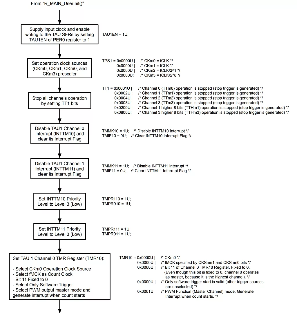
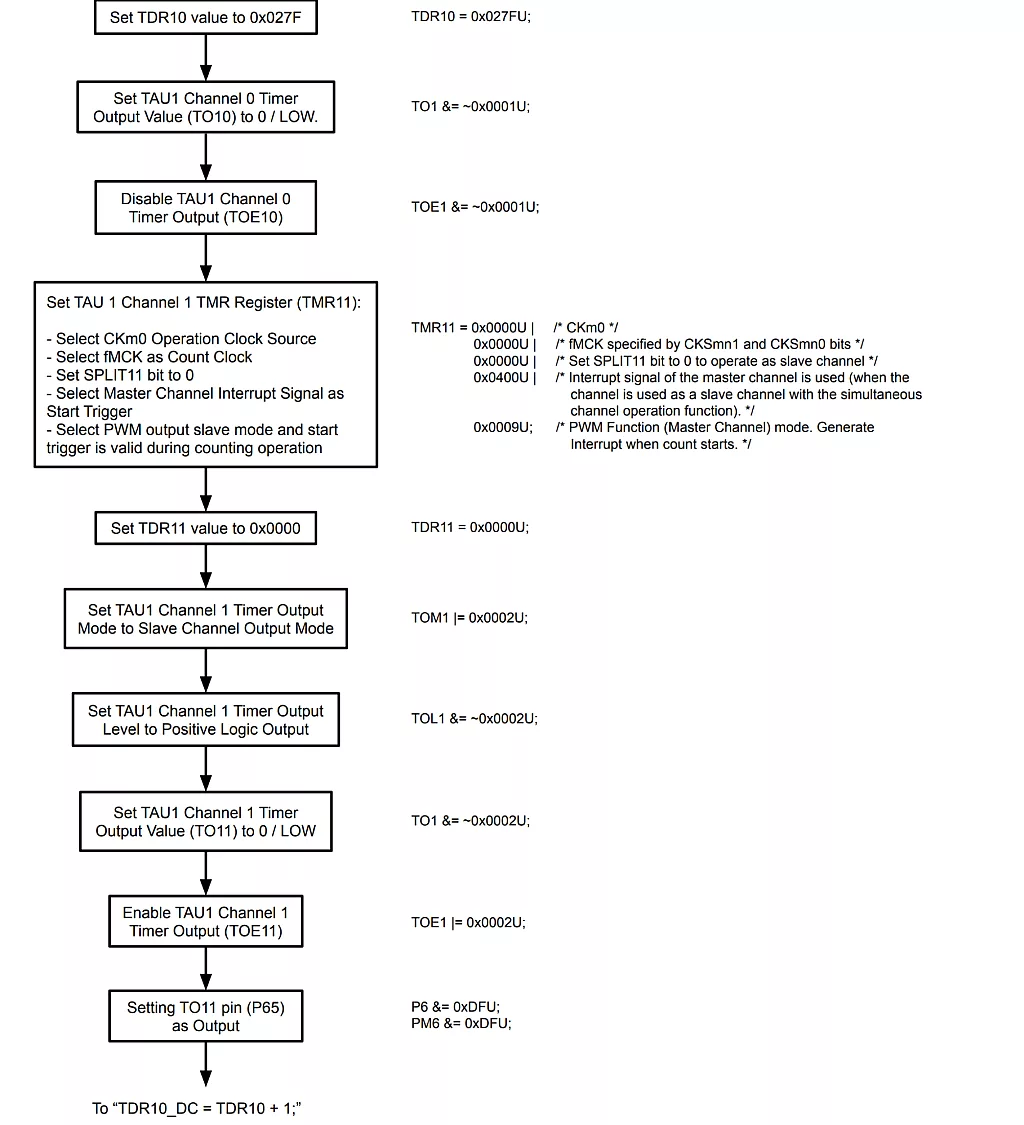
In the initialization, we first set the TAUmEN bit of the PER0 register to 1 to supply the input clock to the TAU and enable writing to the SFRs used by the TAU. We used TAU0 for the delay_us() function. So to avoid conflict, for now, we will use TAU1 for the PWM function and set TAU1EN bit to 1.

Next, we set the prescaler of the operation clock sources (CKm0, CKm1, CKm2, and CKm3) using the TPS1 register. For the PWM function, we can only select CKm0 or CKm1. In our sample project, later,› we will select CKm0. In this case, we can just leave the default value of the bits that set the prescaler of the other operation clock sources (CKm1, CKm2, and CKm3).

In our sample project, we will generate a 50kHz PWM signal (Pulse Period = 1/50kHz = 20us), the minimum frequency recommended for brushless DC motors. We can set the PWM frequency by setting the value of the TDRmn register and the operation clock (CKm0) frequency (see Pulse Period formula in Figure 5). For the CKm0 frequency, 8MHz frequency is enough (PWM resolution = Pulse Period / CKm0 Period = 20us/(1/8MHz) = 160 steps). But to have a better PWM resolution, we can use the maximum frequency, which is 32MHz for the RL78/G14 device used in RL78/G14 FPB (no prescaler used). In this case, we’ll set the PRSm03-PRSm00 bits of the TPS1 register to 0000.

After setting the TPS1 register, we make sure that all TAU1 channels are not operating by setting the bits in the TT1 register. Then we disable the interrupt, clear the interrupt flag, and set the interrupt priority level of TAU1 Channel 0 (Master) and Channel 1 (Slave).

Next, we’re going to set the TMR register of the master channel, TMR10. As discussed in tutorial 7, the TAU of RL78 has three TMR registers. For the master channel, we’re going to use channel 0. So let’s refer to this TMR register:

For the operation clock, we will use CKm0. So we will set the CKSmn1-CKSmn0 bits to 00, and since we’re going to use the operation clock as the count clock, we will set the CCSmn bit to 0. Bit 11 of the channel 0 TMR register is fixed to 0. But since channel 0 is the highest channel, it will always operate as a master. For the start trigger, we will set bits STSmn2-STSmn0 to 000 since we’re going to use a software trigger. For the MDmn3-MDmn0 bits, we will set MDmn3-MDmn1 bits to 000 and MDmn0 to 1 to set the channel operation mode to interval timer/PWM output (master) and to generate an interrupt when counting is started.

That’s all for the master channel TMR register. Next, we set the master channel TDR register, TDR10. The PWM frequency is 50kHz, so the period is 1/50kHz = 20us. We set CKm0 to 32MHz. So each count of the clock is 1/32MHz = 31.25ns. Using the Pulse Period formula in Figure 5, the value that we need to load in the TDR10 register is:

After setting the TDR10 value, we set the timer output value of channel 0 to 0 by setting bit TO10 of the TO1 register to 0 and disable the timer output by setting bit TOE10 of the TOE1 register to 0. We’re going to use the output of the slave, not the master, so we can disable the output of the master channel.

Now, we’re going to set the TMR register of the slave channel, TMR11. The slave channel is channel 1. So let’s refer to this TMR register:

For the operation clock, the slave channel should use the same operation clock that the master channel uses. So we’ll set CKSmn1-CKSmn0 bits to 00 and then set CCSmn bit to 0 to set the slave channel count clock to operation clock. For bit 11, SPLITmn, we’ll set it to 0. This makes the channel a slave in the simultaneous channel operation function. For the STSmn2-STSmn0 bits, we will set them to 100 to set the interrupt signal of the master channel as the start trigger of the slave channel. For the MDmn3-MDmn0 bits, we will set MDmn3-MDmn1 bits to 100 and MDmn0 to 1 to set the channel operation mode to one-count mode/PWM output (slave) to make the start trigger valid during the counting operation.

The value in the TDR register of the slave (TDRmp) controls the duty cycle of the PWM signal (see Figure 5). During the initialization, we can just set the TDRmp value to 0, as we’ll change it anyway later.

After setting TDR11, we’ll set the timer output mode of channel 1 to slave channel output mode by setting the TOMm1 bit of the TOM1 registers to 1. Next, we set the channel 1 timer output level to positive logic by setting the TOLm1 bit of the TOL1 register to 0, and we set the timer output value of channel 1 to 0 or LOW by setting the TOm1 bit of the TO1 register to 0 too.

The slave channel outputs the PWM signal. So we’ll enable the timer output of channel 1 by setting the TOEm1 bit of the TOE1 register to 1 and then set the TO11 pin or pin P65 as output through the P6 and PM6 registers.

So that’s all for the initialization of the TAU PWM function. Here’s the code of the TAU1_PWM_Init() function:
void TAU1_PWM_Init(void)
{
    TAU1EN = 1U;    	/* supplies input clock */

    TPS1 = 0x0000U | 	/* ckm0 - fCLK */
    	 0x0000U | 	/* ckm1 - fCLK */
	 0x0000U | 	/* ckm2 - fCLK/2^1 */
	 0x0000U;	/* ckm2 - fCLK/2^8 */

    /* Stop all channels */
    TT1 = 0x0001U | 		/* Operation stop trigger of channel 0 (TTm0). Operation is stopped (stop trigger is generated). */
               0x0002U | 		/* Operation stop trigger of channel 1 (TTm1). Operation is stopped (stop trigger is generated). */
               0x0004U |		/* Operation stop trigger of channel 2 (TTm2). Operation is stopped (stop trigger is generated). */
               0x0008U | 		/* Operation stop trigger of channel 3 (TTm3). Operation is stopped (stop trigger is generated). */
               0x0200U | 		/* Operation stop trigger of channel 1 higher 8 bits (TTHm1). Operation is stopped (stop trigger is generated). */
               0x0800U;		/* Operation stop trigger of channel 3 higher 8 bits (TTHm3). Operation is stopped (stop trigger is generated). */

    /* Mask channel 0 interrupt */
    TMMK10 = 1U;    /* disable INTTM10 interrupt */
    TMIF10 = 0U;    	/* clear INTTM10 interrupt flag */

    /* Mask channel 1 interrupt */
    TMMK11 = 1U;    /* disable INTTM11 interrupt */
    TMIF11 = 0U;    	/* clear INTTM11 interrupt flag */

    /* Set INTTM10 low priority */
    TMPR110 = 1U;
    TMPR010 = 1U;

    /* Set INTTM11 low priority */
    TMPR111 = 1U;
    TMPR011 = 1U;

    /* Channel 0 is used as master channel for PWM output function */
    TMR10 = 0x0000U | 	/* Selection of macro clock (MCK) of channel n (CKSmn1 - CKSmn0). Operation clock CK0 set by PRS register. */
                    0x0000U | 	/* Selection of count clock (CCK) of channel n (CCSmn). macro clock MCK specified by CKSmn bit. */
                    0x0000U |	/* Selection of slave/master of channel n (MASTERmn). Channel0 operates as master channel. */
                    0x0000U | 	/* Setting of start trigger or capture trigger of channel n (STSmn2 - STSmn0). Only software trigger start is valid. */
                    0x0001U;	/* Operation mode of channel n (MDmn3 - MDmn0). PWM Function (Master Channel) mode. Timer interrupt is generated when counting is started. */

    TDR10 = 0x027FU;
    TO1 &= ~0x0001U;	/* Timer output of channel 0 (TOm0). Set timer output value to 0. */
    TOE1 &= ~0x0001U;	/* Timer output enable/disable of channel 0 (TOEm0). Disable Channel 0 Timer Output. */

    /* Channel 1 is used as slave channel for PWM output function */
    TMR11 = 0x0000U | 	/* Selection of macro clock (MCK) of channel n (CKSmn1 - CKSmn0). Operation clock CK0 set by PRS register. */
                    0x0000U | 	/* Selection of count clock (CCK) of channel n (CCSmn). macro clock MCK specified by CKSmn bit. */
                    0x0000U |	/* Selection of slave/master of channel n (MASTERmn). Operates as slave channel. */
                    0x0400U | 	/* Setting of start trigger or capture trigger of channel n (STSmn2 - STSmn0). Interrupt signal of the master channel is used. */
                    0x0009U;	/* Operation mode of channel n (MDmn3 - MDmn0). PWM Function (Slave Channel) mode. Start trigger is valid during counting operation. */

    TDR11 = 0x0000U;
    TOM1 |= 0x0002U;	/* Control of timer output mode of channel 1 (TOMm1). Combination operation mode. */
    TOL1 &= ~0x0002U;	/* Control of timer output level of channel 1 (TOLm1). Positive logic output (active-high). */
    TO1 &= ~0x0002U;	/* Timer output of channel 1 (TOm1). Set timer output value to 0. */
    TOE1 |= 0x0002U;	/* Timer output enable/disable of channel 1 (TOEm1). Enable Channel 1 Timer Output. */

    /* Set TO11 pin */
    P6 &= 0xDFU;
    PM6 &= 0xDFU;
}
Sample Project
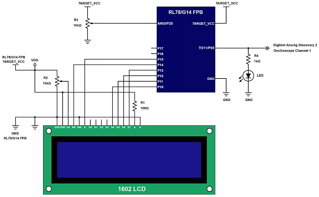
So it’s time to test the PWM function of the TAU. The image below shows the schematic diagram of the sample project we will try. As you can see, we have a potentiometer R3 connected to the ANI0/P20 pin. We’re going to use it to change the duty cycle of the PWM signal. For the output, we’ve connected an LED with a series resistor to pin TO11/P65 so that we’ll have an indicator as we change the duty cycle of the PWM signal. The change in the PWM signal’s duty cycle will change the LED’s brightness. But to see the PWM signal’s width, I’ve also connected the output of the TO11/P65 pin to an oscilloscope. The LCD is just there to display the value read across the analog input ANI0.
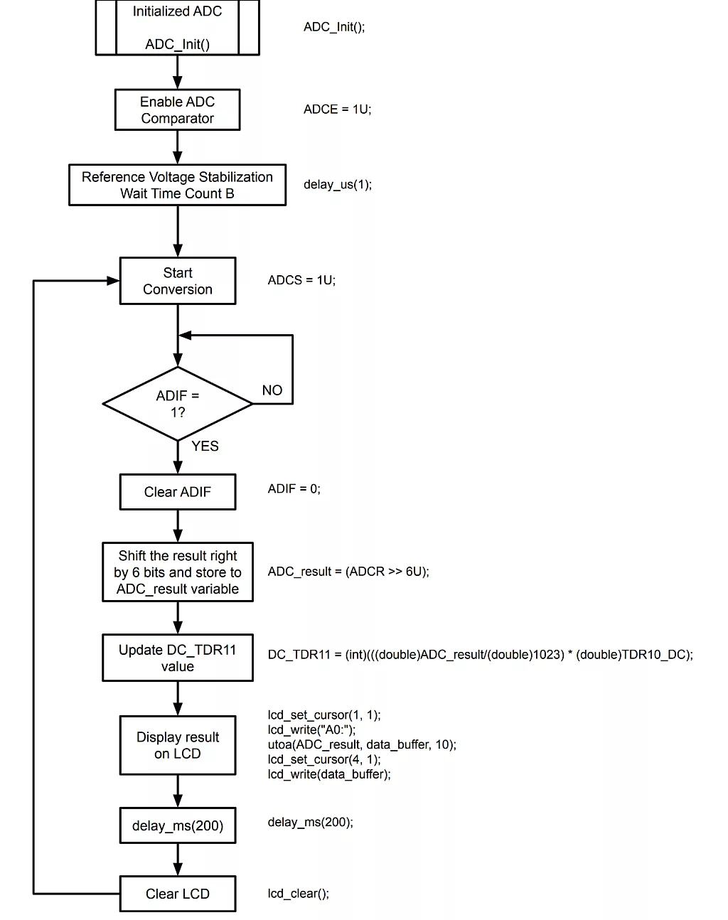
We will follow the process shown in the flowchart below for the code. We will use polling for the ADC. However, for the PWM function, we'll use interrupts for both the master and slave channels. This means that there will be two ISRs. But, we will only use the master channel ISR to update the value of the TDR11 register.
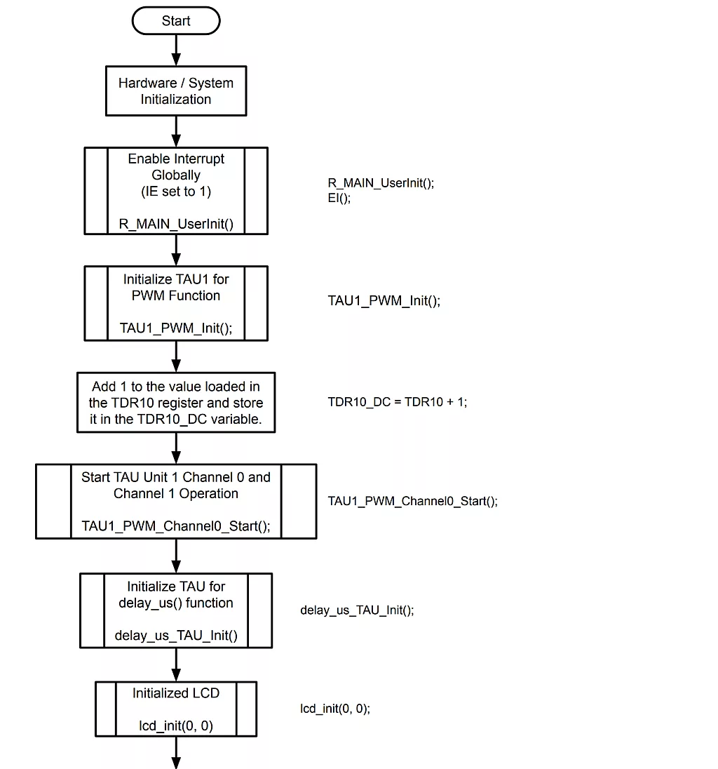
As shown in the flowchart above, the program starts with the hardware/system initialization and then enables maskable interrupts. Next, the program calls the TAU1_PWM_Init() function (line 143 to line 203 of r_main.c) to initialize TAU1 to operate in PWM mode. After initializing the TAU, the program reads the value of the TDR10 register, adds 1 to it, and stores it to the TDR10_DC variable. The TDR10_DC variable will be used later when the program calculates the value to be stored in the TDR11 variable. The program then calls the TAU1_PWM_Channel0_Start() function (line 205 to line 215 of r_main.c) to start generating the PWM signal.
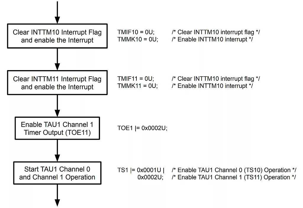
The flowchart below shows the process happening inside the TAU1_PWM_Channel0_Start() function. As you can see, the program clears the interrupt flag of the INTTM10 and the INTTM11 interrupts and enables the interrupts. Then the program enables TAU1 channel 1 timer output and sets the TSm0 and TSm1 bits to 1 to start the operation of TAU1 channel 0 and channel 1. So after executing the TAU1_PWM_Channel0_Start() function, every time the INTTM10 is generated (when counting starts), the program jumps to the master channel ISR, and every time the INTTM11 is generated (when the TDR11 value reaches 0000H), the program jumps to the slave channel ISR.
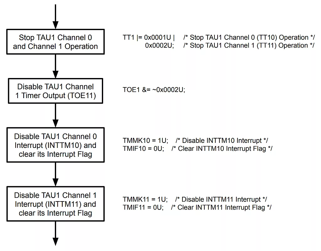
The flowchart below shows the process of the TAU1_PWM_Channel0_Stop() function (line 217 to line 230 of r_main.c), which is the function to call to stop the PWM signal output. However, this function isn’t used or called by the program in the sample project.
After calling the TAU1_PWM_Channel0_Start() function, the program calls the delay_us_TAU_Init() function to initialize TAU0 so we can use the delay_us() function and then calls the lcd_init() function to initialize the LCD. So don’t forget to include the delay and LCD libraries when trying this sample project.

Next, the program calls the ADC_Init() function (line 120 to line 141 of r_main.c) to initialize the ADC to operate in Software Trigger (Select Mode, One-shot Conversion Mode). After initializing the ADC, the program enables the ADC comparator and wait for 1us for the reference voltage to stabilize (Wait Time Count B). Then the program enters the main function infinite loop (line 80 to line 101 of r_main.c).
Inside the infinite loop, the program starts the A/D conversion first and then waits until the ADIF flag becomes 1. After the ADIF flag is set, the program clears the ADIF flag, shifts the A/D conversion result right by 6 bits, then stores the shifted result to the ADC_result_variable.
Next, the program updates the value of the DC_TDR11 variable. This is the formula used to get the new value of the DC_TDR11 variable (line 92 of r_main.c):
The formula is derived from the Duty Factor [%] formula shown in Figure 5. As you can see, the value of the ADC_result variable is divided by 1023. Then whatever the result is, we multiply it by the value of the TDR10_DC variable to get the value to be stored in the TDR register of the slave channel.
When the INTTM10 interrupt is generated, the program jumps to the master channel ISR, TAU1_PWM_Channel0_ISR(), line 232 to line 237 of r_main.c. The value of the TDR11 register is updated by copying the value of the DC_TDR11 variable to the TDR11 register (line 235 of r_main.c).
After updating the value in the DC_TDR11 register, the program displays the digital value equivalent to the analog voltage read by the ADC across the ANI0 input channel. For this kind of example, the LCD is unnecessary. But it’s nice to have a display where we can monitor the analog voltage across the wiper terminal of the potentiometer so we can estimate the duty cycle of the PWM signal.
After a 200ms delay, the program clears the LCD and repeats the whole process inside the infinite loop of the main function.
So here’s the code of the sample project:
/***********************************************************************************************************************
* DISCLAIMER
* This software is supplied by Renesas Electronics Corporation and is only intended for use with Renesas products.
* No other uses are authorized. This software is owned by Renesas Electronics Corporation and is protected under all
* applicable laws, including copyright laws.
* THIS SOFTWARE IS PROVIDED "AS IS" AND RENESAS MAKES NO WARRANTIES REGARDING THIS SOFTWARE, WHETHER EXPRESS, IMPLIED
* OR STATUTORY, INCLUDING BUT NOT LIMITED TO WARRANTIES OF MERCHANTABILITY, FITNESS FOR A PARTICULAR PURPOSE AND
* NON-INFRINGEMENT.  ALL SUCH WARRANTIES ARE EXPRESSLY DISCLAIMED.TO THE MAXIMUM EXTENT PERMITTED NOT PROHIBITED BY
* LAW, NEITHER RENESAS ELECTRONICS CORPORATION NOR ANY OF ITS AFFILIATED COMPANIES SHALL BE LIABLE FOR ANY DIRECT,
* INDIRECT, SPECIAL, INCIDENTAL OR CONSEQUENTIAL DAMAGES FOR ANY REASON RELATED TO THIS SOFTWARE, EVEN IF RENESAS OR
* ITS AFFILIATES HAVE BEEN ADVISED OF THE POSSIBILITY OF SUCH DAMAGES.
* Renesas reserves the right, without notice, to make changes to this software and to discontinue the availability
* of this software. By using this software, you agree to the additional terms and conditions found by accessing the
* following link:
* http://www.renesas.com/disclai...
*
* Copyright (C) 2011, 2021 Renesas Electronics Corporation. All rights reserved.
***********************************************************************************************************************/

/***********************************************************************************************************************
* File Name    : r_main.c
* Version      : CodeGenerator for RL78/G14 V2.05.06.02 [08 Nov 2021]
* Device(s)    : R5F104ML
* Tool-Chain   : GCCRL78
* Description  : This file implements main function.
* Creation Date: 15/02/2023
***********************************************************************************************************************/

/***********************************************************************************************************************
Includes
***********************************************************************************************************************/
#include "r_cg_macrodriver.h"
#include "r_cg_cgc.h"
/* Start user code for include. Do not edit comment generated here */
#include "delay.h"
#include "1602_LCD.h"
/* End user code. Do not edit comment generated here */
#include "r_cg_userdefine.h"

/***********************************************************************************************************************
Global variables and functions
***********************************************************************************************************************/
/* Start user code for global. Do not edit comment generated here */
void ADC_Init(void);
void TAU1_PWM_Init(void);
void TAU1_PWM_Channel0_Start(void);
void TAU1_PWM_Channel0_Stop(void);
void TAU1_PWM_Channel0_ISR(void);
void TAU1_PWM_Channel1_ISR(void);

uint16_t ADC_result = 0;
uint16_t DC_TDR11 = 0;
uint16_t TDR10_DC = 0;
unsigned char data_buffer[100];
/* End user code. Do not edit comment generated here */
void R_MAIN_UserInit(void);

/***********************************************************************************************************************
* Function Name: main
* Description  : This function implements main function.
* Arguments    : None
* Return Value : None
***********************************************************************************************************************/
void main(void)
{
    R_MAIN_UserInit();
    /* Start user code. Do not edit comment generated here */
    TAU1_PWM_Init();
    TDR10_DC = TDR10 + 1;
    TAU1_PWM_Channel0_Start();

    delay_us_TAU_Init();
    lcd_init(0, 0);

    ADC_Init();	/* Initialize ADC */
    		/* If (ADREFP1, ADREFP0) is 00 or 01: Reference Voltage Stabilization Wait Time Count A = No Wait */
    ADCE = 1U;  	/* Enable ADC Comparator */
    delay_us(1);	/* Reference Voltage Stabilization Wait Time Count B */

    while (1U)
    {
        ADCS = 1U;  /* Start ADC Conversion */

        while (ADIF != 1)
        {
            NOP();
        }
        ADIF = 0;

        ADC_result = (ADCR >> 6U);

        DC_TDR11 = (int)(((double)ADC_result/(double)1023) * (double)TDR10_DC);

        lcd_set_cursor(1, 1);
        lcd_write("A0:");
        utoa(ADC_result, data_buffer, 10);
        lcd_set_cursor(4, 1);
        lcd_write(data_buffer);
        delay_ms(200);
        lcd_clear();
    }
    /* End user code. Do not edit comment generated here */
}


/***********************************************************************************************************************
* Function Name: R_MAIN_UserInit
* Description  : This function adds user code before implementing main function.
* Arguments    : None
* Return Value : None
***********************************************************************************************************************/
void R_MAIN_UserInit(void)
{
    /* Start user code. Do not edit comment generated here */
    EI();
    /* End user code. Do not edit comment generated here */
}

/* Start user code for adding. Do not edit comment generated here */
void ADC_Init(void)
{
    ADCEN = 1U;  		/* supply AD clock */
    ADM0 = 0x00U;  		/* disable AD conversion and clear ADM0 register */
    ADMK = 1U;  		/* disable INTAD interrupt */
    ADIF = 0U;  		/* clear INTAD interrupt flag */
    /* The reset status of ADPC is analog input, so it's unnecessary to set. */
    /* Set ANI0 pin as analog input */
    PM2 |= 0x01U;
    ADM0 = 0x00U | 		/* Conversion Clock (fAD): fCLK/64 [FR2-FR0: 000] */
    	  0x00U | 		/* Operating Voltage Mode: Normal 1 [LV1-LV0: 00] */
    	  0x00U;		/* Channel Selection Mode: Select Mode [ADMD = 0] */
    ADM1 = 0x00U |  	/* Trigger Mode: Software [ADTMD1-ADTMD0: 00] */
    	  0x20U;		/* Conversion Operation Mode: One-shot Conversion Mode [ADSCM = 1] */
    ADM2 = 0x00U | 		/* Reference Voltage (+) Side: VDD [ADREFP1-ADREFP0: 00] */
    	  0x00U | 		/* Reference Voltage (-) Side: VSS [ADREFM = 0] */
	  0x00U | 		/* Generates INTAD when ADLL <= ADCRH <= ADUL (AREA 1) [ADRCK = 0] */
	  0x00U;		/* 10-Bit Resolution [ADTYP = 0] */
    ADUL = 0xFFU;		/* Upper Limit Value */
    ADLL = 0x00U;		/* Lower Limit Value */
    ADS = 0x00U;		/* Select ANI0 Channel */
}

void TAU1_PWM_Init(void)
{
    TAU1EN = 1U;    	/* supplies input clock */

    TPS1 = 0x0000U | 	/* ckm0 - fCLK */
    	 0x0000U | 	/* ckm1 - fCLK */
	 0x0000U | 	/* ckm2 - fCLK/2^1 */
	 0x0000U;	/* ckm2 - fCLK/2^8 */

    /* Stop all channels */
    TT1 = 0x0001U | 		/* Operation stop trigger of channel 0 (TTm0). Operation is stopped (stop trigger is generated). */
               0x0002U | 		/* Operation stop trigger of channel 1 (TTm1). Operation is stopped (stop trigger is generated). */
               0x0004U |		/* Operation stop trigger of channel 2 (TTm2). Operation is stopped (stop trigger is generated). */
               0x0008U | 		/* Operation stop trigger of channel 3 (TTm3). Operation is stopped (stop trigger is generated). */
               0x0200U | 		/* Operation stop trigger of channel 1 higher 8 bits (TTHm1). Operation is stopped (stop trigger is generated). */
               0x0800U;		/* Operation stop trigger of channel 3 higher 8 bits (TTHm3). Operation is stopped (stop trigger is generated). */

    /* Mask channel 0 interrupt */
    TMMK10 = 1U;    /* disable INTTM10 interrupt */
    TMIF10 = 0U;    	/* clear INTTM10 interrupt flag */

    /* Mask channel 1 interrupt */
    TMMK11 = 1U;    /* disable INTTM11 interrupt */
    TMIF11 = 0U;    	/* clear INTTM11 interrupt flag */

    /* Set INTTM10 low priority */
    TMPR110 = 1U;
    TMPR010 = 1U;

    /* Set INTTM11 low priority */
    TMPR111 = 1U;
    TMPR011 = 1U;

    /* Channel 0 is used as master channel for PWM output function */
    TMR10 = 0x0000U | 	/* Selection of macro clock (MCK) of channel n (CKSmn1 - CKSmn0). Operation clock CK0 set by PRS register. */
                    0x0000U | 	/* Selection of count clock (CCK) of channel n (CCSmn). macro clock MCK specified by CKSmn bit. */
                    0x0000U |	/* Selection of slave/master of channel n (MASTERmn). Channel0 operates as master channel. */
                    0x0000U | 	/* Setting of start trigger or capture trigger of channel n (STSmn2 - STSmn0). Only software trigger start is valid. */
                    0x0001U;	/* Operation mode of channel n (MDmn3 - MDmn0). PWM Function (Master Channel) mode. Timer interrupt is generated when counting is started. */

    TDR10 = 0x027FU;
    TO1 &= ~0x0001U;	/* Timer output of channel 0 (TOm0). Set timer output value to 0. */
    TOE1 &= ~0x0001U;	/* Timer output enable/disable of channel 0 (TOEm0). Disable Channel 0 Timer Output. */

    /* Channel 1 is used as slave channel for PWM output function */
    TMR11 = 0x0000U | 	/* Selection of macro clock (MCK) of channel n (CKSmn1 - CKSmn0). Operation clock CK0 set by PRS register. */
                    0x0000U | 	/* Selection of count clock (CCK) of channel n (CCSmn). macro clock MCK specified by CKSmn bit. */
                    0x0000U |	/* Selection of slave/master of channel n (MASTERmn). Operates as slave channel. */
                    0x0400U | 	/* Setting of start trigger or capture trigger of channel n (STSmn2 - STSmn0). Interrupt signal of the master channel is used. */
                    0x0009U;	/* Operation mode of channel n (MDmn3 - MDmn0). PWM Function (Slave Channel) mode. Start trigger is valid during counting operation. */

    TDR11 = 0x0000U;
    TOM1 |= 0x0002U;	/* Control of timer output mode of channel 1 (TOMm1). Combination operation mode. */
    TOL1 &= ~0x0002U;	/* Control of timer output level of channel 1 (TOLm1). Positive logic output (active-high). */
    TO1 &= ~0x0002U;	/* Timer output of channel 1 (TOm1). Set timer output value to 0. */
    TOE1 |= 0x0002U;	/* Timer output enable/disable of channel 1 (TOEm1). Enable Channel 1 Timer Output. */

    /* Set TO11 pin */
    P6 &= 0xDFU;
    PM6 &= 0xDFU;
}

void TAU1_PWM_Channel0_Start(void)
{
    TMIF10 = 0U;    	/* clear INTTM10 interrupt flag */
    TMMK10 = 0U;    	/* enable INTTM10 interrupt */
    TMIF11 = 0U;    	/* clear INTTM11 interrupt flag */
    TMMK11 = 0U;    	/* enable INTTM11 interrupt */
    TOE1 |= 0x0002U;	/* Timer output enable/disable of channel 1 (TOEm1). Enable Channel 1 Timer Output. */

    TS1 |= 0x0001U | 	/* Operation enable (start) trigger of channel 0 (TSm0). Operation is enabled (start trigger is generated). */
                0x0002U;		/* Operation enable (start) trigger of channel 1 (TSm1). Operation is enabled (start trigger is generated). */
}

void TAU1_PWM_Channel0_Stop(void)
{
    TT1 |= 0x0001U | 	/* Operation stop trigger of channel 0 (TTm0). Operation is stopped (stop trigger is generated). */
                0x0002U;		/* Operation stop trigger of channel 1 (TTm1). Operation is stopped (stop trigger is generated). */

    TOE1 &= ~0x0002U;	/* Timer output enable/disable of channel 1 (TOEm1). Disable Channel 1 Timer Output.  */

    /* Mask channel 0 interrupt */
    TMMK10 = 1U;    /* disable INTTM10 interrupt */
    TMIF10 = 0U;    	/* clear INTTM10 interrupt flag */
    /* Mask channel 1 interrupt */
    TMMK11 = 1U;    /* disable INTTM11 interrupt */
    TMIF11 = 0U;    	/* clear INTTM11 interrupt flag */
}

void TAU1_PWM_Channel0_ISR(void)
{
    /* Start user code. Do not edit comment generated here */
    TDR11 = DC_TDR11;
    /* End user code. Do not edit comment generated here */
}

void TAU1_PWM_Channel1_ISR(void)
{
    /* Start user code. Do not edit comment generated here */
    /* End user code. Do not edit comment generated here */
}
/* End user code. Do not edit comment generated here */
Since we’re already in tutorial 10, I assume you know howto build the project and upload the code to the RL78/G14 FPB. So I will not discuss the steps anymore. In case you forgot how to create a project, configure some settings, import libraries, etc., please review the previous tutorials.
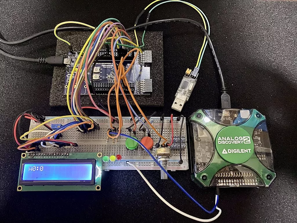
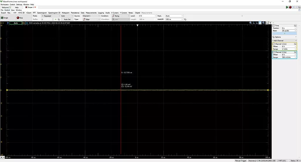
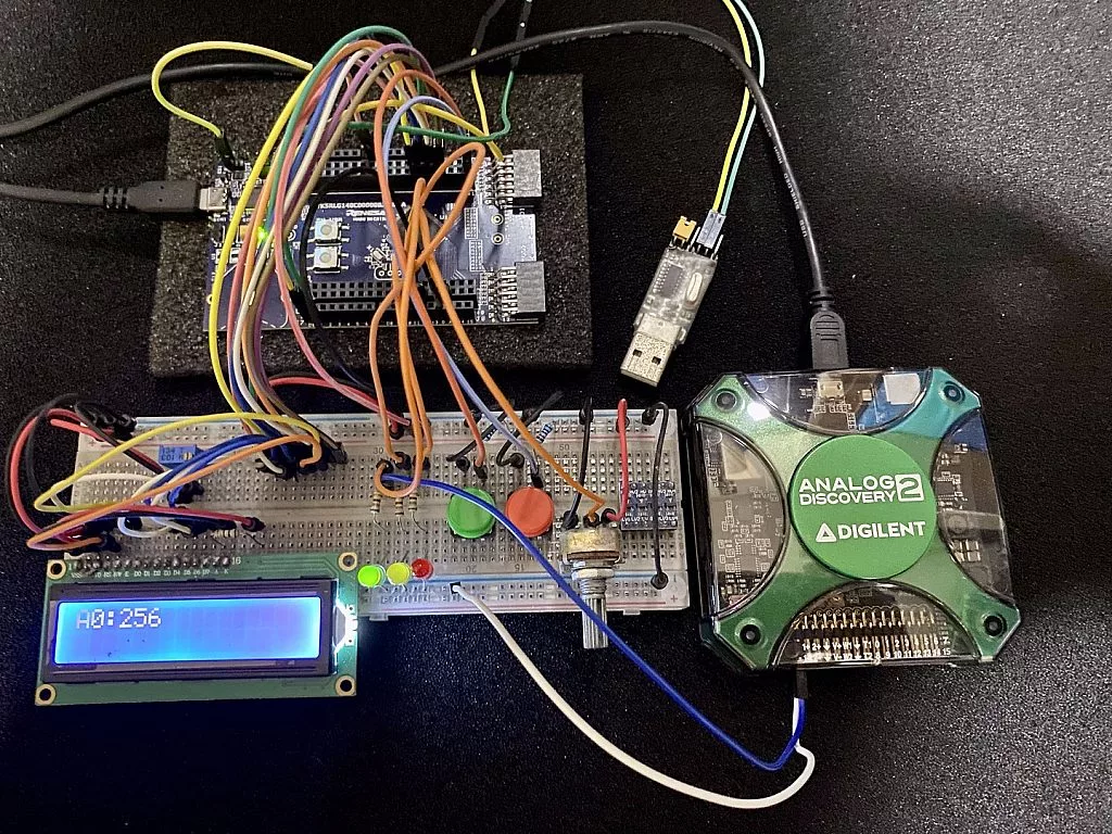
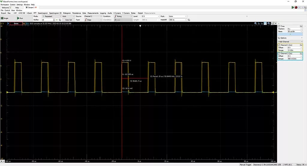
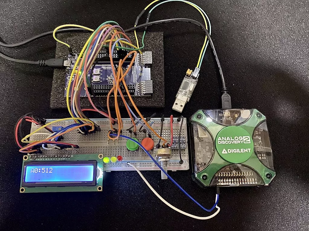
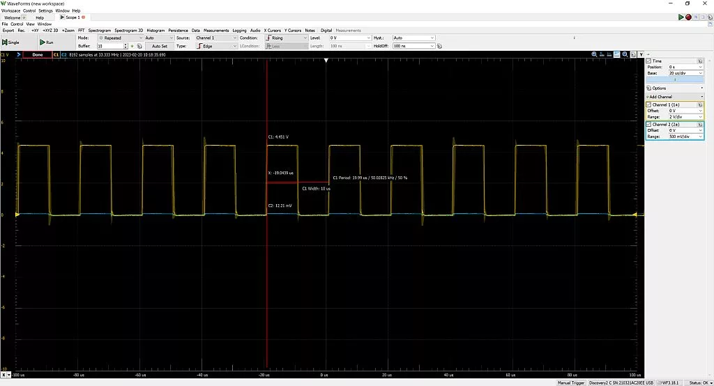
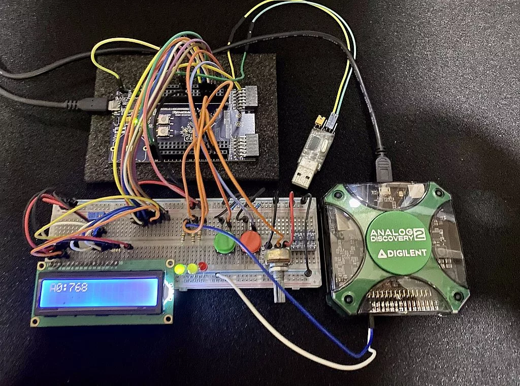
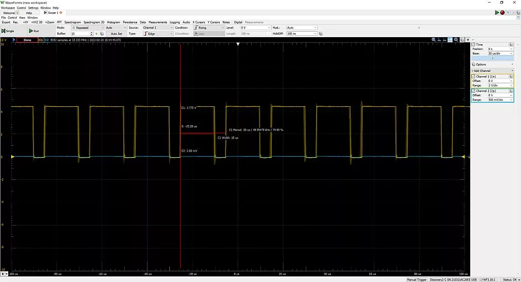
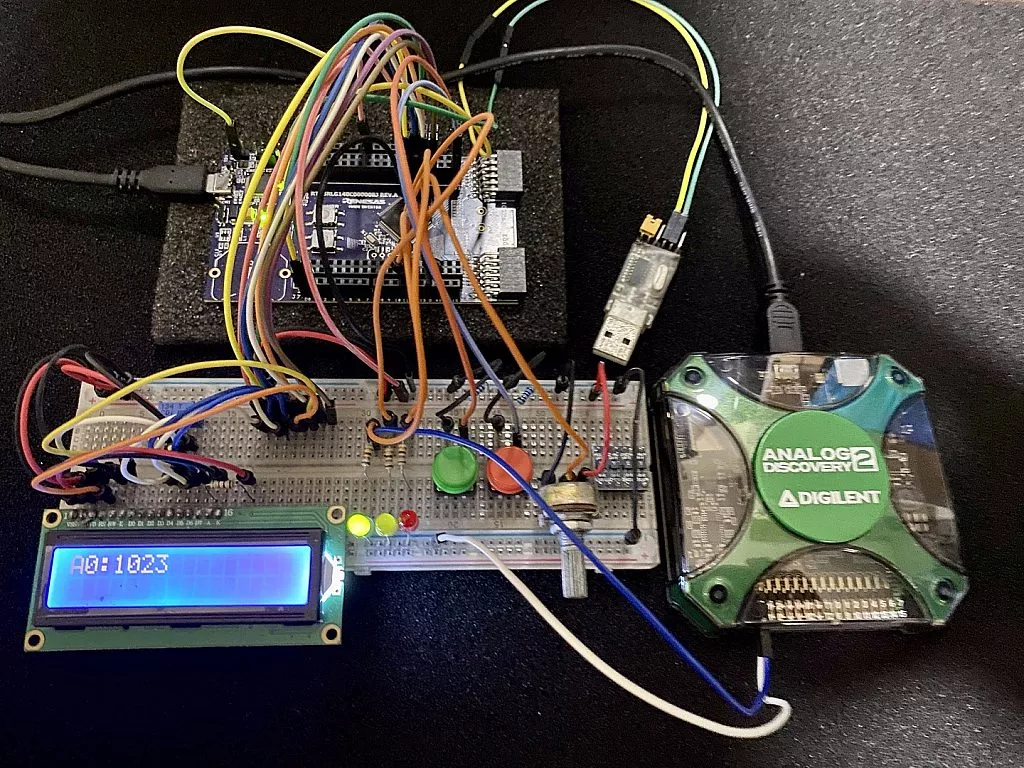
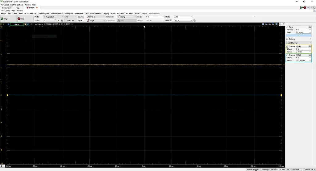
So we’re done! We can now generate a PWM signal using the TAU of the RL78 MCU and can use it in different applications such as motor control, lighting control, voltage regulation, etc. I hope you’ve learned a lot and enjoyed this tutorial. If you have questions, you can leave them in the comments section below, or message us. See you next time!

Get the latest tools and tutorials, fresh from the toaster.


