Understanding Analog-to-Digital Converter (Software Trigger Conversion Modes) | Renesas RL78 - 9
Published
Hi! Welcome back again to CircuitBread. So far, in our previous tutorials, we have only been dealing with digital signals or values which microcontrollers (MCUs) normally work on. However, when it comes to analog signals, MCUs can’t just directly process them. The RL78 MCUs and even other MCUs need a device that will measure the analog signal first and then convert the analog value to a digital value so that the analog signal can be read and processed. This device is called an analog-to-digital converter (ADC) and fortunately, most of the RL78 devices have an internal ADC. So in this tutorial, we will discuss the internal ADC of RL78 MCUs and how we can use it.
RL78 ADC Characteristics
Before we discuss the registers that control the RL78 ADC, let’s first discuss some of its major characteristics.
Conversion Method
There are different types of ADCs. Five major types are delta-sigma (ΔΣ), successive approximation, dual slope, pipelined, and flash ADCs. In the RL78 family, all groups use the successive approximation type except for the RL78/I1B and RL78/I1C which use the delta-sigma type. The RL78/G14 device which we are using in this tutorial series has the successive approximation ADC.
I will not discuss anymore how the successive approximation method works as you can just google it. But these are some of the advantages and disadvantages of the successive approximation method:
Advantages | Disadvantages |
Good Speed/Resolution Ratio | Max Resolution is lower than Delta-Sigma ADC |
Higher Sample Rate than Delta-Sigma ADC | No built-in Anti-Aliasing Filter |
Fixed Conversion Time | Goes all through the steps even if the value was already determined in the previous steps |
Table 1. Successive Approximation ADC Advantage and Disadvantages.
Resolution
The resolution of the ADC is one of the characteristics that determines its step size. The step size is the smallest change in the voltage that can be detected by the ADC. The ADC of the RL78/G14 device can be set to 8 or 10-bit resolution. In the RL78 family, the highest resolution available for devices that use successive approximation ADC is 12-bit while devices with delta-sigma ADC have 24-bit resolution.
Analog Input Channels
The number of analog input channels depends on the number of pins of the RL78 device. In the RL78/G14 devices, devices with lowest pin count (30-pin) have 8 analog input channels while devices with highest pin count (100-pin) have 20 analog input channels. The 80-pin device in the RL78/G14 FPB has 17 analog input channels.

Reference Voltage
Reference voltage, along with the resolution, sets the step size of the ADC. In the RL78 ADC, the positive (+) side of the reference voltage can be supplied from VDD, pin P20/AVREFP/ANI, or from the internal reference voltage (1.45 V) while the negative (-) side of the reference voltage can be supplied from VSS or pin P21/AVREFM/ANI1. Later, we will discuss how to set the reference voltage and the resolution of the RL78 ADC.
Temperature Sensor
This might not be available to some RL78 devices but at least with the RL78/G14 devices, there’s an internal temperature sensor on its ADC that can be selected as an ADC input through the analog input channel specification register (ADS). The output of the temperature sensor at +25°C and its temperature coefficient is shown below.

Operation Voltage Mode
The RL78 ADC has four operating voltage modes: Standard 1 (Normal 1), Standard 2 (Normal 2), Low Voltage 1, and Low Voltage 2. When the operating voltage is between 2.7V and 5.5V (2.7V ≤ VDD ≤ 5.5V), you can set the operation voltage mode to Standard 1 or Standard 2. If the operating voltage is between 1.6V and 5.5V (1.6V ≤ VDD ≤ 5.5V), you can set the operation voltage mode to Low Voltage 1 or Low Voltage 2. The operation voltage mode of the ADC also affects the conversion time of the ADC. So it’s important to know about it.
Sampling and Conversion Time
The sampling time is the time it takes for the sample and hold circuit to sample the analog voltage. It is part of the conversion time. The conversion time is the time from the sampling process up to when the ADC outputs the digital value. The sampling time in Standard 1 or Low Voltage 1 takes 7 fAD (7 cycles of the conversion clock) while Standard 2 or Low Voltage 2 takes 5 fAD. The conversion time of the ADC depends on the CPU and peripheral clock (fCLK) and the FR2-FR0, LV1, and LV0 bits settings in the ADM0 register.

Conversion Modes
In RL78 devices, its ADC has three trigger options to start the conversion, two modes to select the analog input channel/s, and two modes of conversion operation.
For the trigger mode, the options are: software trigger, hardware trigger no-wait, and hardware trigger wait mode. In software trigger mode, the conversion is started by software. In hardware trigger mode, no-wait and wait mode, the conversion is started by detecting a hardware trigger. The difference between hardware trigger no-wait and wait mode is that the wait mode is used when snooze mode function is being used. So in hardware trigger wait mode, there’s an additional time for ADC power supply stabilization.
For the channel selection mode, there are two options: select mode and scan mode. In select mode, the conversion is only performed in one analog input channel while in scan mode, conversion is performed in four consecutive analog input channels (e.g. ANI0-ANI3, ANI1-ANI4, etc.).
For the conversion operation mode, there are also two options: one-shot conversion mode and sequential conversion mode (continuous). In one-shot conversion mode, the conversion is only performed once on the selected analog input channel/s, while in sequential conversion mode, the conversion is performed continuously until it is stopped by software. When scan mode is selected, the conversion is sequentially performed on the four selected channels continuously until the conversion is stopped by software.
So based on the different options in trigger mode, channel selection mode, and conversion operation mode, the RL78 ADC can perform the following conversion modes:
- Software Trigger Mode (Select Mode, Sequential Conversion Mode)
- Software Trigger Mode (Select Mode, One-shot Conversion Mode)
- Software Trigger Mode (Scan Mode, Sequential Conversion Mode)
- Software Trigger Mode (Scan Mode, One-shot Conversion Mode)
- Hardware Trigger No-wait Mode (Select Mode, Sequential Conversion Mode)
- Hardware Trigger No-wait Mode (Select Mode, One-shot Conversion Mode)
- Hardware Trigger No-wait Mode (Scan Mode, Sequential Conversion Mode)
- Hardware Trigger No-wait Mode (Scan Mode, One-shot Conversion Mode)
- Hardware Trigger Wait Mode (Select Mode, Sequential Conversion Mode)
- Hardware Trigger Wait Mode (Select Mode, One-shot Conversion Mode)
- Hardware Trigger Wait Mode (Scan Mode, Sequential Conversion Mode)
- Hardware Trigger Wait Mode (Scan Mode, One-shot Conversion Mode)
However, in this tutorial, we will just focus on the software trigger conversion modes as we have not discussed the other hardware triggers yet.
Registers Controlling ADC
There are 11 registers (not including the register for the interrupt function) that controls the operation of the ADC that we need to familiarize first so that it will be easier for us to understand the examples later. Let’s start with the PER0 register.
Peripheral Enable Register 0 (PER0)
We’re already familiar with the PER0 register as we already discussed its RTCEN, TAU1EN, and TAU0EN bits in the previous tutorials. Now, for the ADC, we will set or clear the ADCEN bit.

Writing 1 to the ADCEN bit enables the clock supply of the ADC. It also enables writing and reading to the SFRs used by the ADC. Clearing the ADCEN bit (set to 0) stops the clock supply of the ADC, disables writing to the ADC SFRs, and puts the ADC in reset status.
A/D Converter Mode Register 0 (ADM0)
There are three A/D converter mode registers: ADM0, ADM1, and ADM2. The ADM0 register is for starting or stopping the conversion and for setting the conversion time. It can be set by a 1-bit or 8-bit memory manipulation instruction. A reset signal clears the ADM0 register to 00H (hex).
 Bits.")
The ADCE bit of the ADM0 register enables the operation of the ADC voltage comparator when set to 1 and stops the operation of the voltage comparator when cleared to 0. Don’t forget to set it to 1 before starting the conversion.
The ADCS bit of the ADM0 register, in software trigger mode, starts the conversion when set to 1 and stops the conversion operation when cleared to 0. The table below shows the settings of the ADCE and ADCS bits and the ADC conversion operation:
ADCE | ADCS | A/D Conversion Operation |
0 | 0 | Conversion Stopped State |
1 | 0 | Conversion Standby State |
0 | 1 | Setting Prohibited |
1 | 1 | Conversion-in-progress State |
Table 4. ADCE and ADCS Bits Settings.
There are some reminders in the hardware user’s manual when setting the ADCE and ADCS bits:
- Do not set the ADCS bit to 1 and the ADCE bit to 0 at the same time.
- Do not change the ADCS and ADCE bits from 0 to 1 at the same time by using an 8-bit manipulation instruction. Be sure to set these bits in the order described in 14.7 A/D Converter Setup Flowchart.

- Note 1. While in the software trigger mode or hardware trigger no-wait mode, the time from the rising of the ADCE bit to the rising of the ADCS bit must be 1us or longer to stabilize the internal circuit.
- Note 2. The following time is the maximum amount of time necessary to start conversion.

Now, let's proceed to the ADMD bit of the ADM0 register. The ADMD bit sets the channel selection mode of the ADC. When set to 0, the channel selection mode is set to select mode. If the ADMD bit is set to 1, the channel selection is set to scan mode.
Bits FR0 to FR2 of the ADM0 register set the conversion time of the ADC while the LV0 and LV1 bits set the operation voltage mode. You can check the different settings of these bits in table 14-3 to table 14-6 of the RL78/G14 hardware user’s manual. We will just show table 14-3 here as we will only use software trigger standard 1 (normal 1) for the examples.
.")
Reminders stated in the hardware user’s manual:
- The above conversion time does not include conversion state time. Conversion state time is added in the first conversion. Select conversion time, taking clock frequency errors into consideration.
- When setting the ADMD, FR2 to FR0, LV1, and LV0 bits, make sure that the conversion is stopped (ADCS = 0, ADCE = 0).
- The A/D conversion time must also be within the relevant range of conversion times (tCONV) described in 34.6.1 or 35.6.1 A/D converter characteristics.
.")
.")
A/D Converter Mode Register 1 (ADM1)
The ADM1 register is used to set the trigger, the conversion operation mode, and the hardware trigger signal. It can be set by a 1-bit or 8-bit memory manipulation instruction and a reset signal clears it to 00H (hex).
 Bits.")
The ADTRS1 and ADTRS0 bits of the ADM1 register select the hardware trigger signal. You can see below the four different hardware trigger signals and the bits settings. However, since we’re just going to use the software trigger mode for now, we can just leave the ADTRS1 and ADTRS0 bits to their default values. In software trigger mode, even if a hardware trigger signal is generated, it will just be ignored.

The ADSCM bit of the ADM1 register sets the conversion operation mode of the ADC. If set to 1, the operation mode is set to one-shot conversion mode while if it’s cleared, the operation mode is set to sequential conversion mode.
The ADTMD1 and ADTMD0 bits of the ADM1 register set the trigger mode. Settings for the trigger are shown below.

When setting the bits in the ADM1 register, make sure that the conversion is stopped (ADCS = 0, ADCE = 0).
A/D Converter Mode Register 2 (ADM2)
The ADM2 register is used to select the (+) positive and (-) negative sides of the ADC reference voltage, check the upper limit and lower limit of the output value of the conversion, select the ADC resolution, and specify whether to use the SNOOZE mode. It can also be set by a 1-bit or 8-bit memory manipulation instruction and a reset signal clears it to 00H (hex).
 Bits.")
The ADTYP bit of the ADM2 register sets the resolution of the RL78 ADC. Setting ADTYP bit to 1 will set the resolution of the ADC to 8-bit while clearing the ADTYP bit will set the resolution to 10-bit.
The AWC bit of the ADM2 register enables (if set to 1) or disables (if set to 0) the ADC SNOOZE mode function. We’re not going to use this in this tutorial, so we’ll just leave its default value (0) later.

The RL78 ADC has two registers that set the upper and lower limits of the conversion result values, ADUL and ADLL, respectively. The ADC generates the interrupt signal (INTAD) at the end of conversion if the value of the ADRCK bit is set to 0 and the output value of the conversion is within the range set by the upper and lower limits. If the value of the ADRCK bit is set to 1, the interrupt signal (INTAD) will only be generated if the conversion output value is greater than the upper limit or less than the lower limit. Please take note that if INTAD does not occur, the conversion result will not be stored.
Now, for the last 3 bits of the ADM2 register, ADREFP1-ADREFP0 bits set the (+) positive side of the reference voltage while the ADREFM bit sets (-) negative side. Check the two tables below for the settings.
 Side Reference Voltage Sources and ADREFP1-ADREFP0 Settings.")
 Side Reference Voltage Sources and ADREFM Settings.")
Reminders from the hardware’s user manual regarding the ADM2 register:
- When setting the ADM2 bits, make sure that conversion is stopped (ADCE = 0, ADCS = 0).
- There are also two stabilization wait times required for the reference voltage. When ADREFP1 and ADREFP0 bits are set to 00 (reference voltage is supplied from VDD) or 01 (reference voltage is supplied from P20/AVREFP/ANI0), reference voltage stabilization wait time (A) is not needed anymore but reference voltage stabilization wait time (B) should be at least 1us. But when ADREFP1 and ADREFP0 bits are set to 10 (reference voltage is supplied from the internal reference voltage), reference voltage stabilization wait time (A) should be at least 5us while reference voltage stabilization wait time (B) is at least 1us.
- When using AVREFP and AVREFM pins, specify ANI0 and ANI1 as the analog input channels and specify input mode by using the port mode register.
10-bit A/D Conversion Result Register (ADCR) and 8-bit A/D Conversion Result Register (ADCRH)
When 10-bit resolution is selected, after the conversion, the 10-bit result from the successive approximation register (SAR) is stored in the ADCR. As you can see below, the ADCR is a 16-bit read-only register which can be read by a 16-bit memory manipulation instruction. The lower 6 bits (bits 0 to 5) of the ADCR are fixed to 0. The result from the SAR is left-justified. The higher 8 bits are stored in bits 8 to 15 of ADCR (address FFF1FH) while the lower 2 bits are stored in bits 6 to 7 of ADCR (address FFF1EH). So when we read the result later, we need to shift the result right by 6 bits to get the correct value.
.")
The ADCRH register below, if you notice, its address is just the same with the higher 8 bits of the ADCR and that’s because it is part of the ADCR. If 8-bit resolution is selected, the 8-bit result is stored in the ADCRH register. In this case, we can just read it. We don’t need to shift the result anymore.
")
Conversion result comparison upper limit setting register (ADUL) and Conversion result comparison lower limit setting register (ADLL)
ADUL and ADLL, these are the registers that are used to set the upper and lower limits of the result of the conversion. Both registers can be set by an 8-bit memory manipulation instruction. However, when a reset signal is generated, the ADUL register is set to FFH (hex) while the ADLL register is cleared to 00H (hex).
As you can see, ADUL and ADLL registers are just 8-bit registers. If 10-bit resolution is selected, only the value stored in the higher 8 bits of the ADCR is compared with the ADUL and ADLL registers.
.")
.")
When setting the ADUL and ADLL registers, make sure that the conversion is stopped (ADCE = 0, ADCS = 1). Also, the setting of the ADUL and ADLL registers must be greater than that of the ADLL register.
A/D Test Register (ADTES)
The ADTES register is used to select the target for conversion. It can be set by an 8-bit memory manipulation instruction and a reset signal clears it to 00H (hex).
.")
The table below shows the different conversion targets and the ADTES bits settings.

When using this register to test the ADC, the hardware’s user manual recommends these settings:
- For zero-scale measurement, select the - side reference voltage as the target for conversion.
- For full-scale measurement, select the + side reference voltage as the target for conversion.
However, for our examples later, we will just be selecting the analog input channels, so we can just leave this register to its default or reset value.
Port Mode Registers 0, 2, 10, 12, 14, and 15 (PM0, PM2, PM10, PM12, PM14, PM15)
In order to set a pin as an analog input, we need to set the PMmn register bit of that pin as an input and set the A/D Port Configuration register (ADPC) for ANI0-ANI14 inputs or the Port Mode Control registers (PMCxx) for ANI16-ANI20 inputs.
A/D Port Configuration Register (ADPC)
The ADPC register is used to switch pins ANI0/P20-ANI7/P27 and ANI8/P150-ANI14/P156 to digital or analog function. It can be set by an 8-bit memory manipulation instruction.
.")
The reset status or value of the ADPC register is 00H (hex). So by default (see table below), the pins ANI0/P20-ANI7/P27 and ANI8/P150-ANI14/P156 act as analog inputs as the reset value of the PMmn registers is FFH (Input Mode).

Another thing to consider here is that we can’t set the pins individually. For example, we can’t set the ANI5/P25 pin as an analog input without setting ANI0/P20-ANI4/P24 as analog inputs too. So, if you’re going to use the ADC, plan first how many analog inputs you need and start from AN0 (if AVREFP and AVREFM are not used for reference voltage) so you can still use the other pins as digital inputs or outputs.
Port Mode Control Registers 0, 10, 12, and 14 (PMC0, PMC10, PMC12, PMC14)
For pins ANI16/P03, ANI17/P02, ANI18/P147, ANI19/P120, and ANI20/P100, these pins can be switched to digital or analog through the PMC registers. The pins can be set as analog inputs by setting their PMC register bit to 1 and they can be set individually.
.")
As shown in the image above, the PMC registers reset value (except PMC1) is FFH (hex). So by default, ANI16-ANI20 pins are analog inputs. The PMC registers can be set by a 1-bit or 8-bit memory manipulation instruction.
Analog Input Channel Specification Register (ADS)
We set pins as analog inputs through the PM, ADPC, and PMC registers. But in selecting the analog input channel/s to be converted, we will use the ADS register. The ADS register can be set by a 1-bit or 8-bit memory manipulation instruction and a reset signal clears it to 00H (hex).
.")
The table below shows the ADS bits settings when the ADMD bit of the ADM0 register is set to 0 (Channel Selection Mode is Select Mode).

If the ADMD bit of the ADM0 register is set to 1 (Channel Selection Mode is Scan Mode), the table below shows the ADS bits settings for selecting four consecutive analog input channels.

Some reminders regarding the ADS register from the hardware’s user manual:
- Rewrite the value of the ADISS bit while conversion is stopped (ADCS = 0, ADCE = 0).
- If AVREFP is used as the (+) side reference voltage of the ADC, do not select ANI0 as the analog input channel.
- If AVREFM is also used as the (-) side reference voltage of the ADC, do not select ANI1 as the analog input channel.
- If the ADISS bit is set to 1, the internal reference voltage (1.45V) cannot be used for the (+) side reference voltage.
ADC Software Trigger Conversion Modes
So we’re done discussing the registers that control the RL78 ADC. Now, we’re going to have one basic example for each of these conversion modes:
- Software Trigger Mode (Select Mode, One-shot Conversion Mode)
- Software Trigger Mode (Select Mode, Sequential Conversion Mode)
- Software Trigger Mode (Scan Mode, One-shot Conversion Mode)
- Software Trigger Mode (Scan Mode, Sequential Conversion Mode).
And for the other settings, please refer to the table below:
Analog Input Channel/s | ANI0/P20 (Select Mode) | ANI0/P20 to ANI3/P23 (Scan Mode) |
Conversion clock (fAD) | fCLK/64 (32MHz/64 = 500kHz or 2us) |
Operating Voltage Mode | Normal 1 |
Reference Voltage (+) Side | VDD |
Reference Voltage (-) Side | VSS |
Generate INTAD Interrupt | when ADLL <= ADCRH <= ADUL (AREA 1) |
ADUL | FFH |
ADLL | 00H |
Table 16. ADC Examples Settings.
For the ADC initialization, we will follow the process shown in the flowchart below. As we jump from one conversion mode to another, we need to change some settings in the initialization function. However, in our examples, the bits or registers that we need to change are just the PM register (for setting analog input channels if changing Channel Selection Mode from Select to Scan Mode), the ADMD bit in ADM0 register (if changing the Channel Selection Mode from Select to Scan Mode), and the ADSCM bit in ADM1 register (if changing the Conversion Operation Mode from One-shot to Sequential). Once we’ve initialized the ADC using the procedure below, we just need to set or clear the ADCE and/or ADCS bits to start and stop the conversion.

We will just use one schematic diagram in all examples (see figure 18). However, in Select Mode examples, we will only use the potentiometer R4 connected to the ANI0/P20 pin. For the Scan Mode examples, we’ll use the four potentiometers R4-R7 connected to pins ANI0/P20-ANI3/P23. The switch S1 will only be used in One-shot Conversion Mode examples. We will display the result/s on the 1602 LCD that we used in the previous tutorial. So let’s start with the Software Trigger Mode (Select Mode, One-shot Conversion Mode) example.

Software Trigger Mode (Select Mode, One-shot Conversion Mode)
The timing diagram below is an example from the hardware user’s manual of the operation timing of the Software Trigger Mode (Select Mode, One-shot Conversion Mode). We are not going to follow it. We will just analyze how the ADC operates in Software Trigger Mode (Select Mode, One-shot Conversion Mode).
 Operation Timing Example.")
As you can see, when the ADCE and ADCS bits are 0, the conversion is in stop status. When the ADCE bit is set to 1 <1>, the ADC is now in conversion standby status. The conversion starts when the ADCS bit is set to 1 <2>. When the conversion ends <3>, the ADCS is automatically cleared <4>, the INTAD interrupt is generated, and the data is stored in the ADCR register. If there are no interruptions such as ADCS being overwritten, ADS rewritten, etc., this is just how the ADC operates in Software Trigger Mode (Select Mode, One-Shot Conversion Mode).
To test this operation, especially the ADCS bit being automatically cleared when the conversion ends, in our example, we will follow the process shown in the flowchart below.
 Example Flowchart.")
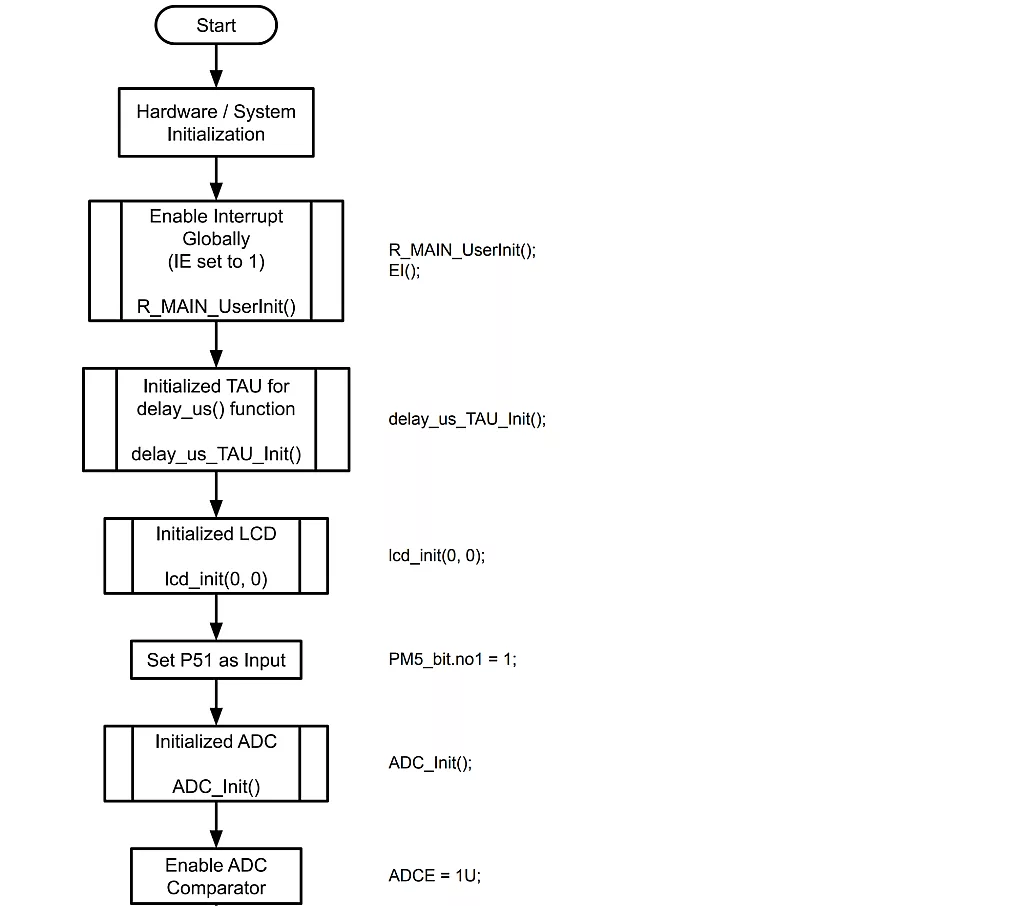
The program starts with the hardware or system initialization. Then we enable interrupts globally by calling the EI() function inside the R_MAIN_UserInit() function. After that, we call the delay_us_TAU_Init() function to initialize the TAU that we’re going to use for the delay_us() function and then call the lcd_init() function to initialize the LCD. We’re going to use the delay functions and the LCD in our examples. So make sure that you always include the delay and LCD libraries in the project. If you forgot how to do this, check the previous tutorials about delays and the 1602 LCD.
After initializing the LCD, we set the pin P51 as input. Then we initialize the ADC by calling the ADC_Init() function. The flowchart below shows the process of initializing the ADC in Software Trigger Mode (Select Mode, One-shot Conversion Mode).
 ADC Initialization Flowchart.")
So based on the flowchart above, these are the steps that we need to follow to initialize the ADC to operate in Software Trigger Mode (Select Mode, One-shot Conversion Mode):
- Set the PER0 ADCEN bit to 1. This enables the ADC clock supply and writing to the SFRs used by the ADC.
- Clear the ADM0 register to make sure that the ADC is in a stopped state (ADCE = 0, ADCS = 0).
- Disable INTAD interrupt and clear its interrupt flag. We’re not using the interrupt function of the ADC here so we mask the ADMK flag and clear the ADIF flag.
- We should set the ADPC register here but since the reset value of the ADPC makes all pins of Port 2 analog inputs and since we’re not going to use the other pins of Port 2 as digital I/Os, we don’t need to set it anymore.
- Set the PM2 register to make pin P20 an analog input. We’re going to use bitwise operator OR here so we will not affect the other pins.
- Set FR2-FR0, LV1-LV0, and ADMD bits of the ADM0 register.
- Set FR2-FR0 to 000 to set the ADC conversion clock to fCLK/64.
- Set LV1-LV0 to 00 to set the operating voltage mode to Normal 1.
- Set ADMD to 0 to operate in Select Mode.
- Set ADTMD1-ADTMD0 and ADSCM bits of the AMD1 register.
- Set ADTMD1-ADTMD0 to 00 to select Software Trigger Mode.
- Set ADSCM to 1 to operate in One-shot Conversion Mode.
- Set ADREFP1-ADREFP0, ADREFM, ADRCK, and ADTYP bits of the ADM2 register.
- Set ADREFP1-ADREFP0 to 00 to set the (+) side of the reference voltage to VDD.
- Set ADREFM to 0 to set the (-) side of the reference voltage to VSS.
- Set ADRCK to 0 to generate interrupt when ADLL <= ADCRH <= ADUL.
- Set ADTYP to 0 to set the ADC’s resolution to 10-bit.
- Set the value of ADUL to FFH.
- Set the value of ADLL to 00H.
- Set ADS register to 00H to select ANI0 as analog input channel.
So this is the code of the ADC_Init() function for Software Trigger Mode (Select Mode, One-shot Conversion Mode) based on the steps mentioned above:
void ADC_Init(void)
{
   ADCEN = 1U;  	    /* supply AD clock */
   ADM0 = 0x00U;  	    /* disable AD conversion and clear ADM0 register */
   ADMK = 1U;  	    /* disable INTAD interrupt */
   ADIF = 0U;  	    /* clear INTAD interrupt flag */
   /* The reset status of ADPC is analog input, so it's unnecessary to set. */
   /* Set ANI0 pin as analog input */
   PM2 |= 0x01U;
   ADM0 = 0x00U | 	    /* Conversion Clock (fAD): fCLK/64 [FR2-FR0: 000] */
   0x00U | 	    /* Operating Voltage Mode: Normal 1 [LV1-LV0: 00] */
   0x00U;	    /* Channel Selection Mode: Select Mode [ADMD = 0] */
   ADM1 = 0x00U |      /* Trigger Mode: Software [ADTMD1-ADTMD0: 00] */
   0x20U;	    /* Conversion Operation Mode: One-shot Conversion Mode [ADSCM = 1] */
   ADM2 = 0x00U | 	    /* Reference Voltage (+) Side: VDD [ADREFP1-ADREFP0: 00] */
   0x00U | 	    /* Reference Voltage (-) Side: VSS [ADREFM = 0] */
   0x00U | 	    /* Generates INTAD when ADLL <= ADCRH <= ADUL (AREA 1) [ADRCK = 0] */
   0x00U;	    /* 10-Bit Resolution [ADTYP = 0] */
   ADUL = 0xFFU;	    /* Upper Limit Value */
   ADLL = 0x00U;	    /* Lower Limit Value */
   ADS = 0x00U;	    /* Select ANI0 Channel */
}
After we initialize the ADC, we’re going to enable the ADC voltage comparator by setting the ADCE bit of the ADM0 register to 1. This will make the ADC enter into standby status and all we need to do for the conversion to start is to set the ADCS bit of the ADM0 register to 1.
 Example Flowchart Infinite Loop.")
As shown in the flowchart of our example, after enabling the comparator, the program enters an infinite loop. Inside this loop, the program checks first if the switch S1 is pressed (P5_bit.no1 = 0) or not (P5_bit.no1 = 1). If the switch is not pressed, the program will just display the recent value stored in the ADC_result variable and then check the status of the switch again.
Now, if the switch is pressed, after generating a 200ms delay and clearing the LCD, the program starts the analog to digital conversion by setting the ADCS bit to 1. Since we’re not using the interrupt function of the ADC here, we will poll the ADIF bit to know if the conversion is already done. When the value of the ADIF bit becomes 1, this means that the conversion is done. Actually, we can also poll the ADCS bit as it is cleared automatically when the conversion ends.
When the conversion ends, we clear the ADIF bit, shift the result of the conversion right by 6 bits and then store it to the ADC_result variable. The value of the ADC_result value will be displayed on the LCD and the program will check the status of the switch again.
So here’s the code of the Software Trigger Mode (Select Mode, One-shot Conversion Mode) example:
/***********************************************************************************************************************
* DISCLAIMER
* This software is supplied by Renesas Electronics Corporation and is only intended for use with Renesas products.
* No other uses are authorized. This software is owned by Renesas Electronics Corporation and is protected under all
* applicable laws, including copyright laws.
* THIS SOFTWARE IS PROVIDED "AS IS" AND RENESAS MAKES NO WARRANTIES REGARDING THIS SOFTWARE, WHETHER EXPRESS, IMPLIED
* OR STATUTORY, INCLUDING BUT NOT LIMITED TO WARRANTIES OF MERCHANTABILITY, FITNESS FOR A PARTICULAR PURPOSE AND
* NON-INFRINGEMENT.  ALL SUCH WARRANTIES ARE EXPRESSLY DISCLAIMED.TO THE MAXIMUM EXTENT PERMITTED NOT PROHIBITED BY
* LAW, NEITHER RENESAS ELECTRONICS CORPORATION NOR ANY OF ITS AFFILIATED COMPANIES SHALL BE LIABLE FOR ANY DIRECT,
* INDIRECT, SPECIAL, INCIDENTAL OR CONSEQUENTIAL DAMAGES FOR ANY REASON RELATED TO THIS SOFTWARE, EVEN IF RENESAS OR
* ITS AFFILIATES HAVE BEEN ADVISED OF THE POSSIBILITY OF SUCH DAMAGES.
* Renesas reserves the right, without notice, to make changes to this software and to discontinue the availability
* of this software. By using this software, you agree to the additional terms and conditions found by accessing the
* following link:
* http://www.renesas.com/disclai...
*
* Copyright (C) 2011, 2021 Renesas Electronics Corporation. All rights reserved.
***********************************************************************************************************************/

/***********************************************************************************************************************
* File Name    : r_main.c
* Version      : CodeGenerator for RL78/G14 V2.05.06.02 [08 Nov 2021]
* Device(s)    : R5F104ML
* Tool-Chain   : GCCRL78
* Description  : This file implements main function.
* Creation Date: 18/01/2023
***********************************************************************************************************************/

/***********************************************************************************************************************
Includes
***********************************************************************************************************************/
#include "r_cg_macrodriver.h"
#include "r_cg_cgc.h"
/* Start user code for include. Do not edit comment generated here */
#include "delay.h"
#include "1602_LCD.h"
/* End user code. Do not edit comment generated here */
#include "r_cg_userdefine.h"

/***********************************************************************************************************************
Global variables and functions
***********************************************************************************************************************/
/* Start user code for global. Do not edit comment generated here */
void ADC_Init(void);
uint16_t ADC_result = 0;
unsigned char data_buffer[100];
/* End user code. Do not edit comment generated here */
void R_MAIN_UserInit(void);

/***********************************************************************************************************************
* Function Name: main
* Description  : This function implements main function.
* Arguments    : None
* Return Value : None
***********************************************************************************************************************/
void main(void)
{
    R_MAIN_UserInit();
    /* Start user code. Do not edit comment generated here */
    delay_us_TAU_Init();
    lcd_init(0, 0);
    PM5_bit.no1 = 1;

    ADC_Init();	/* Initialize ADC */
    		/* If (ADREFP1, ADREFP0) is 00 or 01: Reference Voltage Stabilization Wait Time Count A = No Wait */
    ADCE = 1U;  	/* Enable ADC Comparator */

    while (1U)
    {
        if (P5_bit.no1 == 0)
        {
            delay_ms(200);

            lcd_clear();

            ADCS = 1U;  /* Start ADC Conversion */

            while (ADIF != 1)
            {
                NOP();
            }
            ADIF = 0;

            ADC_result = (ADCR >> 6U);
        }

        lcd_set_cursor(1, 1);
        lcd_write("A0:");
        utoa(ADC_result, data_buffer, 10);
        lcd_set_cursor(4, 1);
        lcd_write(data_buffer);
    }
    /* End user code. Do not edit comment generated here */
}


/***********************************************************************************************************************
* Function Name: R_MAIN_UserInit
* Description  : This function adds user code before implementing main function.
* Arguments    : None
* Return Value : None
***********************************************************************************************************************/
void R_MAIN_UserInit(void)
{
    /* Start user code. Do not edit comment generated here */
    EI();
    /* End user code. Do not edit comment generated here */
}

/* Start user code for adding. Do not edit comment generated here */
void ADC_Init(void)
{
    ADCEN = 1U;  	    /* supply AD clock */
    ADM0 = 0x00U;  	    /* disable AD conversion and clear ADM0 register */
    ADMK = 1U;  	    /* disable INTAD interrupt */
    ADIF = 0U;  	    /* clear INTAD interrupt flag */
    /* The reset status of ADPC is analog input, so it's unnecessary to set. */
    /* Set ANI0 pin as analog input */
    PM2 |= 0x01U;
    ADM0 = 0x00U | 	    /* Conversion Clock (fAD): fCLK/64 [FR2-FR0: 000] */
    	  0x00U | 	    /* Operating Voltage Mode: Normal 1 [LV1-LV0: 00] */
    	  0x00U;	    /* Channel Selection Mode: Select Mode [ADMD = 0] */
    ADM1 = 0x00U |      /* Trigger Mode: Software [ADTMD1-ADTMD0: 00] */
                  0x20U;	    /* Conversion Operation Mode: One-shot Conversion Mode [ADSCM = 1] */
    ADM2 = 0x00U | 	    /* Reference Voltage (+) Side: VDD [ADREFP1-ADREFP0: 00] */
                  0x00U | 	    /* Reference Voltage (-) Side: VSS [ADREFM = 0] */
                  0x00U | 	    /* Generates INTAD when ADLL <= ADCRH <= ADUL (AREA 1) [ADRCK = 0] */
    	  0x00U;	    /* 10-Bit Resolution [ADTYP = 0] */
    ADUL = 0xFFU;	    /* Upper Limit Value */
    ADLL = 0x00U;	    /* Lower Limit Value */
    ADS = 0x00U;	    /* Select ANI0 Channel */
}
/* End user code. Do not edit comment generated here */
Again, when creating the project and generating code for the system initialization, don’t forget to enable the fSUB clock and disable the watchdog timer. Don’t forget to include the delay and 1602 LCD libraries too. When debugging, don’t forget to disable Power Target From The Emulator (MAX 200mA). Now, upload the code to the RL78/G14 FPB and test it by tweaking the potentiometer R4 and pressing the switch S1.
 Example Output.")
Software Trigger Mode (Select Mode, Sequential Conversion Mode)
We’re done with the Software Trigger Mode (Select Mode, One-shot Conversion Mode) example. For the Software Trigger Mode (Select Mode, Sequential Conversion Mode) example, let’s check the timing diagram below.
 Operation Timing Example.")
As you can see, the operation is just similar to the One-Shot Conversion Mode. The conversion starts when we set the ADCS bit to 1, the operation is interrupted by rewriting the ADCS bit or the ADS register to change the analog input channel, etc. Their only difference is that, in Sequential Conversion Mode, the ADCS bit is not automatically cleared when the conversion ends.
So to test this, in our example, we’ll follow the process shown in the flowchart below. In this example, we will use the interrupt function of the ADC.
 Example Flowchart.")
For the initialization, as shown above, it’s similar to the first example. We initialize the hardware/system, enable the global interrupt, initialize the TAU, the LCD, and the ADC. But this time, we will not set P51 as input as we will not use a switch in this example. For the ADC initialization, let’s check the flowchart below.
 ADC Initialization Flowchart.")
Since we’re not going to change anything except the Conversion Operation Mode, the initialization will just be similar to the initialization in One-shot Conversion Mode, except that we will clear the ADSCM bit of the ADM1 register to choose Sequential Conversion Mode. So here’s the code of the ADC_Init() function for the Software Trigger Mode (Select Mode, Sequential Conversion Mode) operation:
void ADC_Init(void)
{
    ADCEN = 1U;  	    /* supply AD clock */
    ADM0 = 0x00U;  	    /* disable AD conversion and clear ADM0 register */
    ADMK = 1U;  	    /* disable INTAD interrupt */
    ADIF = 0U;  	    /* clear INTAD interrupt flag */
    /* The reset status of ADPC is analog input, so it's unnecessary to set. */
    /* Set ANI0 pin as analog input */
    PM2 |= 0x01U;
    ADM0 = 0x00U | 	    /* Conversion Clock (fAD): fCLK/64 [FR2-FR0: 000] */
    	  0x00U | 	    /* Operating Voltage Mode: Normal 1 [LV1-LV0: 00] */
    	  0x00U;	    /* Channel Selection Mode: Select Mode [ADMD = 0] */
    ADM1 = 0x00U |      /* Trigger Mode: Software [ADTMD1-ADTMD0: 00] */
    	  0x00U;	    /* Conversion Operation Mode: Sequential Conversion Mode [ADSCM = 0] */
    ADM2 = 0x00U | 	    /* Reference Voltage (+) Side: VDD [ADREFP1-ADREFP0: 00] */
    	  0x00U | 	    /* Reference Voltage (-) Side: VSS [ADREFM = 0] */
    	  0x00U | 	    /* Generates INTAD when ADLL <= ADCRH <= ADUL (AREA 1) [ADRCK = 0] */
    	  0x00U;	    /* 10-Bit Resolution [ADTYP = 0] */
    ADUL = 0xFFU;	    /* Upper Limit Value */
    ADLL = 0x00U;	    /* Lower Limit Value */
    ADS = 0x00U;	    /* Select ANI0 Channel */
}
After the ADC initialization, we will enable the ADC voltage comparator (set ADCE to 1) and then wait for 1us for the stabilization of the reference voltage. If you notice, Reference Voltage Stabilization Wait Time Count A is not present in this example. It’s also not present in the other three examples. This is because our reference voltage is supplied from VDD and VSS and Wait Time Count A is not needed anymore. However, for Reference Voltage Stabilization Wait Time Count B, we also didn’t include it in the previous example as we didn’t immediately start the conversion in the previous example. There’s enough time for the reference voltage to stabilize after enabling the comparator. In this example, as shown in the flowchart, we included the Reference Voltage Stabilization Wait Time Count B as we will immediately start the conversion by software (set ADCS to 1) after enabling the comparator (set ADCE to 1) and its interrupt (set ADMK and ADIF to 0).
 Example Infinite Loop.")
So after setting ADCS to 1 to start the conversion, the program will now enter an infinite loop and inside this loop, the program will just display the result on the LCD and update it every 2 seconds. But maybe you’re wondering, where’s the part where we shift the result right by 6 bits and store it on a variable? I’ve put it inside the ISR of the ADC. I don’t need to discuss how to set up the interrupt as we already discussed it in this tutorial: Renesas RL78 - 5. Interrupt Functions. If you forgot how to do it, just review tutorial 5.
 Example ISR Flowchart.")
When the conversion ends, the program jumps to the ISR of the ADC. The flowchart above shows what’s inside the ISR. As you can see, the first thing that the program does here is mask the interrupt and clear the interrupt flag so that we won’t receive another interrupt request while we are shifting the result and storing it to the ADC_result variable. After the result is stored in the ADC_result variable, we enable the interrupt again and the program returns inside the infinite loop and updates the LCD again with the new result.
 Example Output.")
So in this example, we can see that in Sequential Conversion Mode, the ADCS bit is not really cleared automatically after the conversion unlike in the One-shot Conversion Mode. The ADC will keep on converting the analog signal from the input channel unless we clear the ADCS bit. So upload the code below to the RL78/G14 FPB, tweak the potentiometer R4, and you’ll see the result on the LCD being updated every 2 seconds.
/***********************************************************************************************************************
* DISCLAIMER
* This software is supplied by Renesas Electronics Corporation and is only intended for use with Renesas products.
* No other uses are authorized. This software is owned by Renesas Electronics Corporation and is protected under all
* applicable laws, including copyright laws.
* THIS SOFTWARE IS PROVIDED "AS IS" AND RENESAS MAKES NO WARRANTIES REGARDING THIS SOFTWARE, WHETHER EXPRESS, IMPLIED
* OR STATUTORY, INCLUDING BUT NOT LIMITED TO WARRANTIES OF MERCHANTABILITY, FITNESS FOR A PARTICULAR PURPOSE AND
* NON-INFRINGEMENT.  ALL SUCH WARRANTIES ARE EXPRESSLY DISCLAIMED.TO THE MAXIMUM EXTENT PERMITTED NOT PROHIBITED BY
* LAW, NEITHER RENESAS ELECTRONICS CORPORATION NOR ANY OF ITS AFFILIATED COMPANIES SHALL BE LIABLE FOR ANY DIRECT,
* INDIRECT, SPECIAL, INCIDENTAL OR CONSEQUENTIAL DAMAGES FOR ANY REASON RELATED TO THIS SOFTWARE, EVEN IF RENESAS OR
* ITS AFFILIATES HAVE BEEN ADVISED OF THE POSSIBILITY OF SUCH DAMAGES.
* Renesas reserves the right, without notice, to make changes to this software and to discontinue the availability
* of this software. By using this software, you agree to the additional terms and conditions found by accessing the
* following link:
* http://www.renesas.com/disclai...
*
* Copyright (C) 2011, 2021 Renesas Electronics Corporation. All rights reserved.
***********************************************************************************************************************/

/***********************************************************************************************************************
* File Name    : r_main.c
* Version      : CodeGenerator for RL78/G14 V2.05.06.02 [08 Nov 2021]
* Device(s)    : R5F104ML
* Tool-Chain   : GCCRL78
* Description  : This file implements main function.
* Creation Date: 18/01/2023
***********************************************************************************************************************/

/***********************************************************************************************************************
Includes
***********************************************************************************************************************/
#include "r_cg_macrodriver.h"
#include "r_cg_cgc.h"
/* Start user code for include. Do not edit comment generated here */
#include "delay.h"
#include "1602_LCD.h"
/* End user code. Do not edit comment generated here */
#include "r_cg_userdefine.h"

/***********************************************************************************************************************
Global variables and functions
***********************************************************************************************************************/
/* Start user code for global. Do not edit comment generated here */
void ADC_Init(void);
void ADC_ISR(void);
volatile uint16_t ADC_result = 0;
unsigned char data_buffer[100];
/* End user code. Do not edit comment generated here */
void R_MAIN_UserInit(void);

/***********************************************************************************************************************
* Function Name: main
* Description  : This function implements main function.
* Arguments    : None
* Return Value : None
***********************************************************************************************************************/
void main(void)
{
    R_MAIN_UserInit();
    /* Start user code. Do not edit comment generated here */
    delay_us_TAU_Init();
    lcd_init(0, 0);

    ADC_Init();	/* Initialize ADC */
    		/* If (ADREFP1, ADREFP0) is 00 or 01: Reference Voltage Stabilization Wait Time Count A = No Wait */
    ADCE = 1U;  	/* Enable ADC Comparator */
    delay_us(1);	/* Reference Voltage Stabilization Wait Time Count B */
    ADMK = 0U;  	/* Enable INTAD interrupt */
    ADIF = 0U;  	/* clear INTAD interrupt flag */
    ADCS = 1U;  	/* Start ADC Conversion */

    while (1U)
    {
        lcd_set_cursor(1, 1);
        lcd_write("A0:");
        utoa(ADC_result, data_buffer, 10);
        lcd_set_cursor(4, 1);
        lcd_write(data_buffer);

        delay_ms(2000);
        lcd_clear();
    }
    /* End user code. Do not edit comment generated here */
}


/***********************************************************************************************************************
* Function Name: R_MAIN_UserInit
* Description  : This function adds user code before implementing main function.
* Arguments    : None
* Return Value : None
***********************************************************************************************************************/
void R_MAIN_UserInit(void)
{
    /* Start user code. Do not edit comment generated here */
    EI();
    /* End user code. Do not edit comment generated here */
}

/* Start user code for adding. Do not edit comment generated here */
void ADC_Init(void)
{
    ADCEN = 1U;  	    /* supply AD clock */
    ADM0 = 0x00U;  	    /* disable AD conversion and clear ADM0 register */
    ADMK = 1U;  	    /* disable INTAD interrupt */
    ADIF = 0U;  	    /* clear INTAD interrupt flag */
    /* The reset status of ADPC is analog input, so it's unnecessary to set. */
    /* Set ANI0 pin as analog input */
    PM2 |= 0x01U;
    ADM0 = 0x00U | 	    /* Conversion Clock (fAD): fCLK/64 [FR2-FR0: 000] */
    	  0x00U | 	    /* Operating Voltage Mode: Normal 1 [LV1-LV0: 00] */
    	  0x00U;	    /* Channel Selection Mode: Select Mode [ADMD = 0] */
    ADM1 = 0x00U |      /* Trigger Mode: Software [ADTMD1-ADTMD0: 00] */
    	  0x00U;	    /* Conversion Operation Mode: Sequential Conversion Mode [ADSCM = 0] */
    ADM2 = 0x00U | 	    /* Reference Voltage (+) Side: VDD [ADREFP1-ADREFP0: 00] */
    	  0x00U | 	    /* Reference Voltage (-) Side: VSS [ADREFM = 0] */
    	  0x00U | 	    /* Generates INTAD when ADLL <= ADCRH <= ADUL (AREA 1) [ADRCK = 0] */
    	  0x00U;	    /* 10-Bit Resolution [ADTYP = 0] */
    ADUL = 0xFFU;	    /* Upper Limit Value */
    ADLL = 0x00U;	    /* Lower Limit Value */
    ADS = 0x00U;	    /* Select ANI0 Channel */
}

void ADC_ISR(void)
{
    ADMK = 1U;  	/* disable INTAD interrupt */
    ADIF = 0U;  	/* clear INTAD interrupt flag */

    ADC_result = (ADCR >> 6U);

    ADMK = 0U;  	/* Enable INTAD interrupt */
    ADIF = 0U;  	/* clear INTAD interrupt flag */
}
/* End user code. Do not edit comment generated here */
Software Trigger Mode (Scan Mode, One-shot Conversion Mode)
We’re done with the two Select Mode examples. The remaining two examples will be both Scan Mode. This means that we’re now going to use four analog input channels, ANI0/P20 to ANI3/P23 pins. This example is One-shot Conversion Mode, so we will use the switch S1 again. Let’s check the timing diagram below for the Software Trigger Mode (Scan Mode, One-shot Conversion Mode) operation.
 Operation Timing Example.")
The operation of the ADC in Software Trigger Mode (Scan Mode, One-shot Conversion Mode) is just similar to how it operates in Software Trigger Mode (Select Mode, One-shot Conversion Mode). The ADCS bit is automatically cleared when the conversion ends. However, this is Scan Mode. So the conversion ends after the ADC is done converting the four analog input signals. If the ADC is not yet done converting all the analog inputs and the conversion is interrupted, the partially converted data will be discarded.
Another important thing to take note here is that INTAD is generated and the result is stored in the ADCR register each time the ADC is done converting an analog input. This means INTAD will be generated four times and the ADCR register value will be updated four times too each time we write 1 to the ADCS bit. In this case, we need to store the result to another variable each time the ADC is done converting an input or else, we’ll just get the value from the 4th analog input channel.
So in our example, we’ll follow the flowchart below. We will use the switch S1 for starting the conversion, the four potentiometers R4-R7 as inputs, and the LCD to display the results. We will not use the interrupt function of ADC just like in the Select Mode One-shot Conversion Mode example. We will just poll the ADIF bit.
 Example Flowchart.")
For the initialization part, everything is the same as what we saw in the Select Mode One-shot Conversion Mode example. From the hardware/system initialization up to ADC initialization. However, we will make some changes in the ADC_Init() function. Let’s check the flowchart below.
 ADC Initialization Flowchart.")
Since we will use four analog input channels, we will change the PM2 register. We use PM2 |= 0x01U; in Select Mode as we only need the ANI0/P20 pin. We will change this to PM2 |= 0x0FU; so that we can set pins ANI0/P20 to ANI3/P23 as inputs. In the ADM0 register, we will set the ADMD bit to 1 to set the Channel Selection Mode into Scan Mode. We don’t need to change the ADS register anymore as 0x00 selects ANI0-ANI3. So here’s the code of the ADC_Init() function for Scan Mode One-shot Conversion Mode:
void ADC_Init(void)
{
    ADCEN = 1U;  	    /* supply AD clock */
    ADM0 = 0x00U;  	    /* disable AD conversion and clear ADM0 register */
    ADMK = 1U;  	    /* disable INTAD interrupt */
    ADIF = 0U;  	    /* clear INTAD interrupt flag */
    /* The reset status of ADPC is analog input, so it's unnecessary to set. */
    /* Set ANI0-ANI3 pins as analog inputs */
    PM2 |= 0x0FU;
    ADM0 = 0x00U | 	    /* Conversion Clock (fAD): fCLK/64 [FR2-FR0: 000] */
    	  0x00U | 	    /* Operating Voltage Mode: Normal 1 [LV1-LV0: 00] */
	  0x40U;	    /* Channel Selection Mode: Scan Mode [ADMD = 1] */
    ADM1 = 0x00U |      /* Trigger Mode: Software [ADTMD1-ADTMD0: 00] */
    	  0x20U;	    /* Conversion Operation Mode: One-shot Conversion Mode [ADSCM = 1] */
    ADM2 = 0x00U | 	    /* Reference Voltage (+) Side: VDD [ADREFP1-ADREFP0: 00] */
    	  0x00U | 	    /* Reference Voltage (-) Side: VSS [ADREFM = 0] */
	  0x00U | 	    /* Generates INTAD when ADLL <= ADCRH <= ADUL (AREA 1) [ADRCK = 0] */
	  0x00U;	    /* 10-Bit Resolution [ADTYP = 0] */
    ADUL = 0xFFU;	    /* Upper Limit Value */
    ADLL = 0x00U;	    /* Lower Limit Value */
    ADS = 0x00U;	    /* Select ANI0-ANI3 Channel */
}
After initializing the ADC, we enable the ADC voltage comparator and now the program enters an infinite loop.
 Example Infinite Loop.")
Just like in the Select Mode One-shot Conversion Mode example, as the program enters the infinite loop, the first thing it checks is if the switch S1 is pressed (P5_bit.no1 = 0) or not (P5_bit.no1 = 1). If the switch S1 is not pressed, the program will just then display the values recently stored in the array ADC_result[]. I used an array here that can store 4 elements to store the results from the four analog input channels.
When the switch S1 is pressed, the program starts the conversion after generating a 200ms delay, initializing the variable i to 0, and clearing the LCD. Then the program enters another loop inside the infinite loop.

Inside this loop, the program checks the value of i. Initially, the value of i is 0. As the ADC converts the input and stores the result to the array ADC_result[i], the value of i is incremented. After converting all four inputs, the value of i becomes 4 and the program exits the loop and displays the results on the LCD.
Here’s the code for this example:
/***********************************************************************************************************************
* DISCLAIMER
* This software is supplied by Renesas Electronics Corporation and is only intended for use with Renesas products.
* No other uses are authorized. This software is owned by Renesas Electronics Corporation and is protected under all
* applicable laws, including copyright laws.
* THIS SOFTWARE IS PROVIDED "AS IS" AND RENESAS MAKES NO WARRANTIES REGARDING THIS SOFTWARE, WHETHER EXPRESS, IMPLIED
* OR STATUTORY, INCLUDING BUT NOT LIMITED TO WARRANTIES OF MERCHANTABILITY, FITNESS FOR A PARTICULAR PURPOSE AND
* NON-INFRINGEMENT.  ALL SUCH WARRANTIES ARE EXPRESSLY DISCLAIMED.TO THE MAXIMUM EXTENT PERMITTED NOT PROHIBITED BY
* LAW, NEITHER RENESAS ELECTRONICS CORPORATION NOR ANY OF ITS AFFILIATED COMPANIES SHALL BE LIABLE FOR ANY DIRECT,
* INDIRECT, SPECIAL, INCIDENTAL OR CONSEQUENTIAL DAMAGES FOR ANY REASON RELATED TO THIS SOFTWARE, EVEN IF RENESAS OR
* ITS AFFILIATES HAVE BEEN ADVISED OF THE POSSIBILITY OF SUCH DAMAGES.
* Renesas reserves the right, without notice, to make changes to this software and to discontinue the availability
* of this software. By using this software, you agree to the additional terms and conditions found by accessing the
* following link:
* http://www.renesas.com/disclai...
*
* Copyright (C) 2011, 2021 Renesas Electronics Corporation. All rights reserved.
***********************************************************************************************************************/

/***********************************************************************************************************************
* File Name    : r_main.c
* Version      : CodeGenerator for RL78/G14 V2.05.06.02 [08 Nov 2021]
* Device(s)    : R5F104ML
* Tool-Chain   : GCCRL78
* Description  : This file implements main function.
* Creation Date: 19/01/2023
***********************************************************************************************************************/

/***********************************************************************************************************************
Includes
***********************************************************************************************************************/
#include "r_cg_macrodriver.h"
#include "r_cg_cgc.h"
/* Start user code for include. Do not edit comment generated here */
#include "delay.h"
#include "1602_LCD.h"
/* End user code. Do not edit comment generated here */
#include "r_cg_userdefine.h"

/***********************************************************************************************************************
Global variables and functions
***********************************************************************************************************************/
/* Start user code for global. Do not edit comment generated here */
void ADC_Init(void);
uint16_t ADC_result[4];
unsigned char data_buffer[100];
/* End user code. Do not edit comment generated here */
void R_MAIN_UserInit(void);

/***********************************************************************************************************************
* Function Name: main
* Description  : This function implements main function.
* Arguments    : None
* Return Value : None
***********************************************************************************************************************/
void main(void)
{
    R_MAIN_UserInit();
    /* Start user code. Do not edit comment generated here */
    delay_us_TAU_Init();
    lcd_init(0, 0);
    PM5_bit.no1 = 1;

    ADC_Init();	/* Initialize ADC */
    		/* If (ADREFP1, ADREFP0) is 00 or 01: Reference Voltage Stabilization Wait Time Count A = No Wait */
    ADCE = 1U;  	/* Enable ADC Comparator */

    while (1U)
    {
        if (P5_bit.no1 == 0)
        {
            delay_ms(200);

            uint8_t i = 0;

            lcd_clear();

            ADCS = 1U;  /* Start ADC Conversion */

            while (i<4)
            {
            	while (ADIF != 1)
    	{
    	    NOP();
    	}
    	ADIF = 0;

    	ADC_result[i] = (ADCR >> 6U);

    	i++;
            }
        }

        lcd_set_cursor(1, 1);
        lcd_write("A0:");
        utoa(ADC_result[0], data_buffer, 10);
        lcd_set_cursor(4, 1);
        lcd_write(data_buffer);

        lcd_set_cursor(9, 1);
        lcd_write("A1:");
        utoa(ADC_result[1], data_buffer, 10);
        lcd_set_cursor(12, 1);
        lcd_write(data_buffer);

        lcd_set_cursor(1, 2);
        lcd_write("A2:");
        utoa(ADC_result[2], data_buffer, 10);
        lcd_set_cursor(4, 2);
        lcd_write(data_buffer);

        lcd_set_cursor(9, 2);
        lcd_write("A3:");
        utoa(ADC_result[3], data_buffer, 10);
        lcd_set_cursor(12, 2);
        lcd_write(data_buffer);
    }
    /* End user code. Do not edit comment generated here */
}


/***********************************************************************************************************************
* Function Name: R_MAIN_UserInit
* Description  : This function adds user code before implementing main function.
* Arguments    : None
* Return Value : None
***********************************************************************************************************************/
void R_MAIN_UserInit(void)
{
    /* Start user code. Do not edit comment generated here */
    EI();
    /* End user code. Do not edit comment generated here */
}

/* Start user code for adding. Do not edit comment generated here */
void ADC_Init(void)
{
    ADCEN = 1U;  	    /* supply AD clock */
    ADM0 = 0x00U;  	    /* disable AD conversion and clear ADM0 register */
    ADMK = 1U;  	    /* disable INTAD interrupt */
    ADIF = 0U;  	    /* clear INTAD interrupt flag */
    /* The reset status of ADPC is analog input, so it's unnecessary to set. */
    /* Set ANI0-ANI3 pins as analog inputs */
    PM2 |= 0x0FU;
    ADM0 = 0x00U | 	    /* Conversion Clock (fAD): fCLK/64 [FR2-FR0: 000] */
    	  0x00U | 	    /* Operating Voltage Mode: Normal 1 [LV1-LV0: 00] */
	  0x40U;	    /* Channel Selection Mode: Scan Mode [ADMD = 1] */
    ADM1 = 0x00U |      /* Trigger Mode: Software [ADTMD1-ADTMD0: 00] */
    	  0x20U;	    /* Conversion Operation Mode: One-shot Conversion Mode [ADSCM = 1] */
    ADM2 = 0x00U | 	    /* Reference Voltage (+) Side: VDD [ADREFP1-ADREFP0: 00] */
    	  0x00U | 	    /* Reference Voltage (-) Side: VSS [ADREFM = 0] */
	  0x00U | 	    /* Generates INTAD when ADLL <= ADCRH <= ADUL (AREA 1) [ADRCK = 0] */
	  0x00U;	    /* 10-Bit Resolution [ADTYP = 0] */
    ADUL = 0xFFU;	    /* Upper Limit Value */
    ADLL = 0x00U;	    /* Lower Limit Value */
    ADS = 0x00U;	    /* Select ANI0-ANI3 Channel */
}
/* End user code. Do not edit comment generated here */
 Example Output.")
Upload it to the RL78/FPB. Tweak the potentiometers R4-R7 and press the switch. The results will be displayed on the LCD. Now let’s proceed to the last example.
Software Trigger Mode (Scan Mode, Sequential Conversion Mode)
For our last example, we’re going to have Sequential Conversion Mode. But this time, in Scan Mode. So the ADC will convert four analog inputs and just like in our 2nd example, which uses Sequential Conversion Mode, the ADCS bit will not be automatically cleared when conversion ends.
 Operation Timing Example.")
As you can see in the timing diagram above, the ADC starts the next conversion right after a conversion ends. The conversion will only stop if we clear the ADCS bit through software instruction. Now, let’s check the flowchart of the example.
 Example Flowchart.")
 Example Flowchart.")
The initialization part, from the system to the ADC, is just the same in the 2nd example and we’re also not going to use the switch here. For the ADC initialization (check flowchart below), it is just similar to our previous (3rd) example. We only need to change the ADSCM bit to 0 to change the Conversion Operation Mode from One-shot to Sequential Conversion Mode.
 ADC Initialization Flowchart.")
So here’s the code of the ADC_Init() function for Scan Mode Sequential Conversion Mode:
void ADC_Init(void)
{
    ADCEN = 1U;  	    /* supply AD clock */
    ADM0 = 0x00U;  	    /* disable AD conversion and clear ADM0 register */
    ADMK = 1U;  	    /* disable INTAD interrupt */
    ADIF = 0U;  	    /* clear INTAD interrupt flag */
    /* The reset status of ADPC is analog input, so it's unnecessary to set. */
    /* Set ANI0-ANI3 pins as analog inputs */
    PM2 |= 0x0FU;
    ADM0 = 0x00U | 	    /* Conversion Clock (fAD): fCLK/64 [FR2-FR0: 000] */
    	  0x00U | 	    /* Operating Voltage Mode: Normal 1 [LV1-LV0: 00] */
	  0x40U;	    /* Channel Selection Mode: Scan Mode [ADMD = 1] */
    ADM1 = 0x00U |      /* Trigger Mode: Software [ADTMD1-ADTMD0: 00] */
    	  0x00U;	    /* Conversion Operation Mode: Sequential Conversion Mode [ADSCM = 0] */
    ADM2 = 0x00U | 	    /* Reference Voltage (+) Side: VDD [ADREFP1-ADREFP0: 00] */
    	  0x00U | 	    /* Reference Voltage (-) Side: VSS [ADREFM = 0] */
	  0x00U | 	    /* Generates INTAD when ADLL <= ADCRH <= ADUL (AREA 1) [ADRCK = 0] */
	  0x00U;	    /* 10-Bit Resolution [ADTYP = 0] */
    ADUL = 0xFFU;	    /* Upper Limit Value */
    ADLL = 0x00U;	    /* Lower Limit Value */
    ADS = 0x00U;	    /* Select ANI0-ANI3 Channel */
}
After the ADC initialization, we enable the ADC voltage comparator, wait for 1us (Reference Voltage Stabilization Wait Time Count B), enable the ADC interrupt, and clear the interrupt flag. But we will not start the conversion yet. The conversion starts when the program enters the infinite loop.
As shown in the flowchart above, after starting the conversion, the program will wait for the value of i to become 4 before it proceeds to the other instructions. The variable i here was declared as a global variable and was initialized to 0. Its value will be incremented inside the ISR of the ADC.
 Example ISR Flowchart.")
The flowchart above shows the operation inside the ISR of the ADC and the first thing the program does here is disable the interrupt and clear the interrupt flag. Then it shifts the result right by 6 bits, stores it in the ADC_result[i] array, and increments the value of i. After that, the program enables the interrupt again and clears the interrupt flag. Then it jumps back to the main infinite loop. The conversion ends after executing this process four times and the value of i is now 4. So the program exits the loop inside the infinite loop and proceeds to the next instruction which is to clear the ADCS bit to make the ADC in standby status.
Now, after clearing the ADCS bit, the program displays the results on the LCD. Then after a 2000ms delay, it clears the display, sets the value of i to 0 again, and starts the conversion again by setting ADCS bit to 1.
 Example Output.")
So we’re done! Try uploading the code below to the RL78/G14 FPB and tweak the potentiometers R4-R7. The values displayed on the LCD will be updated every 2 seconds.
/***********************************************************************************************************************
* DISCLAIMER
* This software is supplied by Renesas Electronics Corporation and is only intended for use with Renesas products.
* No other uses are authorized. This software is owned by Renesas Electronics Corporation and is protected under all
* applicable laws, including copyright laws.
* THIS SOFTWARE IS PROVIDED "AS IS" AND RENESAS MAKES NO WARRANTIES REGARDING THIS SOFTWARE, WHETHER EXPRESS, IMPLIED
* OR STATUTORY, INCLUDING BUT NOT LIMITED TO WARRANTIES OF MERCHANTABILITY, FITNESS FOR A PARTICULAR PURPOSE AND
* NON-INFRINGEMENT.  ALL SUCH WARRANTIES ARE EXPRESSLY DISCLAIMED.TO THE MAXIMUM EXTENT PERMITTED NOT PROHIBITED BY
* LAW, NEITHER RENESAS ELECTRONICS CORPORATION NOR ANY OF ITS AFFILIATED COMPANIES SHALL BE LIABLE FOR ANY DIRECT,
* INDIRECT, SPECIAL, INCIDENTAL OR CONSEQUENTIAL DAMAGES FOR ANY REASON RELATED TO THIS SOFTWARE, EVEN IF RENESAS OR
* ITS AFFILIATES HAVE BEEN ADVISED OF THE POSSIBILITY OF SUCH DAMAGES.
* Renesas reserves the right, without notice, to make changes to this software and to discontinue the availability
* of this software. By using this software, you agree to the additional terms and conditions found by accessing the
* following link:
* http://www.renesas.com/disclai...
*
* Copyright (C) 2011, 2021 Renesas Electronics Corporation. All rights reserved.
***********************************************************************************************************************/

/***********************************************************************************************************************
* File Name    : r_main.c
* Version      : CodeGenerator for RL78/G14 V2.05.06.02 [08 Nov 2021]
* Device(s)    : R5F104ML
* Tool-Chain   : GCCRL78
* Description  : This file implements main function.
* Creation Date: 19/01/2023
***********************************************************************************************************************/

/***********************************************************************************************************************
Includes
***********************************************************************************************************************/
#include "r_cg_macrodriver.h"
#include "r_cg_cgc.h"
/* Start user code for include. Do not edit comment generated here */
#include "delay.h"
#include "1602_LCD.h"
/* End user code. Do not edit comment generated here */
#include "r_cg_userdefine.h"

/***********************************************************************************************************************
Global variables and functions
***********************************************************************************************************************/
/* Start user code for global. Do not edit comment generated here */
void ADC_Init(void);
void ADC_ISR(void);
volatile uint16_t ADC_result[4];
unsigned char data_buffer[100];
volatile uint8_t i = 0;
/* End user code. Do not edit comment generated here */
void R_MAIN_UserInit(void);

/***********************************************************************************************************************
* Function Name: main
* Description  : This function implements main function.
* Arguments    : None
* Return Value : None
***********************************************************************************************************************/
void main(void)
{
    R_MAIN_UserInit();
    /* Start user code. Do not edit comment generated here */
    delay_us_TAU_Init();
    lcd_init(0, 0);

    ADC_Init();	/* Initialize ADC */
    		/* If (ADREFP1, ADREFP0) is 00 or 01: Reference Voltage Stabilization Wait Time Count A = No Wait */
    ADCE = 1U;  	/* Enable ADC Comparator */
    delay_us(1);
    ADMK = 0U;  	/* Enable INTAD interrupt */
    ADIF = 0U;  	/* clear INTAD interrupt flag */

    while (1U)
    {
        ADCS = 1U;  /* Start ADC Conversion */

        while (i < 4)
        {
            NOP();
        }

        ADCS = 0U;  /* Stop ADC Conversion */

        lcd_set_cursor(1, 1);
        lcd_write("AO:");
        utoa(ADC_result[0], data_buffer, 10);
        lcd_set_cursor(4, 1);
        lcd_write(data_buffer);

        lcd_set_cursor(9, 1);
        lcd_write("A1:");
        utoa(ADC_result[1], data_buffer, 10);
        lcd_set_cursor(12, 1);
        lcd_write(data_buffer);

        lcd_set_cursor(1, 2);
        lcd_write("A2:");
        utoa(ADC_result[2], data_buffer, 10);
        lcd_set_cursor(4, 2);
        lcd_write(data_buffer);

        lcd_set_cursor(9, 2);
        lcd_write("A3:");
        utoa(ADC_result[3], data_buffer, 10);
        lcd_set_cursor(12, 2);
        lcd_write(data_buffer);

        delay_ms(2000);
        lcd_clear();
        i = 0;
    }
    /* End user code. Do not edit comment generated here */
}


/***********************************************************************************************************************
* Function Name: R_MAIN_UserInit
* Description  : This function adds user code before implementing main function.
* Arguments    : None
* Return Value : None
***********************************************************************************************************************/
void R_MAIN_UserInit(void)
{
    /* Start user code. Do not edit comment generated here */
    EI();
    /* End user code. Do not edit comment generated here */
}

/* Start user code for adding. Do not edit comment generated here */
void ADC_Init(void)
{
    ADCEN = 1U;  	    /* supply AD clock */
    ADM0 = 0x00U;  	    /* disable AD conversion and clear ADM0 register */
    ADMK = 1U;  	    /* disable INTAD interrupt */
    ADIF = 0U;  	    /* clear INTAD interrupt flag */
    /* The reset status of ADPC is analog input, so it's unnecessary to set. */
    /* Set ANI0-ANI3 pins as analog inputs */
    PM2 |= 0x0FU;
    ADM0 = 0x00U | 	    /* Conversion Clock (fAD): fCLK/64 [FR2-FR0: 000] */
    	  0x00U | 	    /* Operating Voltage Mode: Normal 1 [LV1-LV0: 00] */
	  0x40U;	    /* Channel Selection Mode: Scan Mode [ADMD = 1] */
    ADM1 = 0x00U |      /* Trigger Mode: Software [ADTMD1-ADTMD0: 00] */
    	  0x00U;	    /* Conversion Operation Mode: Sequential Conversion Mode [ADSCM = 0] */
    ADM2 = 0x00U | 	    /* Reference Voltage (+) Side: VDD [ADREFP1-ADREFP0: 00] */
    	  0x00U | 	    /* Reference Voltage (-) Side: VSS [ADREFM = 0] */
	  0x00U | 	    /* Generates INTAD when ADLL <= ADCRH <= ADUL (AREA 1) [ADRCK = 0] */
	  0x00U;	    /* 10-Bit Resolution [ADTYP = 0] */
    ADUL = 0xFFU;	    /* Upper Limit Value */
    ADLL = 0x00U;	    /* Lower Limit Value */
    ADS = 0x00U;	    /* Select ANI0-ANI3 Channel */
}

void ADC_ISR(void)
{
    ADMK = 1U;  	/* disable INTAD interrupt */
    ADIF = 0U;  	/* clear INTAD interrupt flag */

    ADC_result[i] = (ADCR >> 6U);

    i++;

    ADMK = 0U;  	/* Enable INTAD interrupt */
    ADIF = 0U;  	/* clear INTAD interrupt flag */
}
/* End user code. Do not edit comment generated here */
Finally, we are done! We can now use the ADC of the RL78 to measure analog signals. I’ll probably add more ADC related examples in the next tutorials. But I hope you’ve learned a lot and hopefully you’ve enjoyed this tutorial. If you have questions, you can leave it in the comments section below or you can message us. See you next time!

Authored By
JB Magoncia
JB is an Electronics Engineer who is interested in audio, embedded systems, and PCB design. He is one of CircuitBread Engineers. JB is also a musician who mainly plays piano/keyboard but can also play bass, guitar, and drums. He currently lives in Cagayan de Oro, Philippines.

Related Tutorials

Related EE FAQs
 work?")
How do Analog to Digital Converters (ADCs) work?

Answered by Uma Bharathi D

What is the Difference Between Analog and Digital Signal Processing?

Answered by Amrutha Varshini
Explore CircuitBread
- 244 Tutorials
- 9 Textbooks
- 12 Study Guides
- 31 Tools
- 104 EE FAQs
- 295 Equations Library
- 213 Reference Materials
- 97 Glossary of Terms
Friends of CircuitBread
-

Free Educational Blog Content
-

Check Out Our Free Ohm's Law Calculator
-

Free YouTube Product Training Guides


Get the latest tools and tutorials, fresh from the toaster.


