- Electromagnetics I
- Ch 3
- Loc 3.11
Microstrip Line
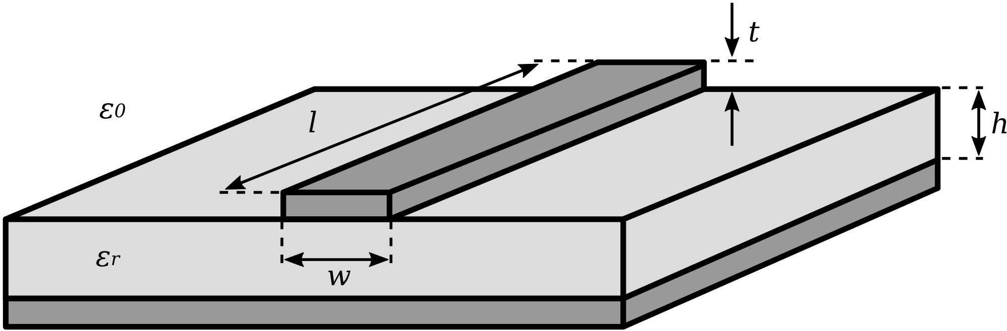
A microstrip transmission line consists of a narrow metallic trace separated from a metallic ground plane by a slab of dielectric material, as shown in Figure 3.11.1. This is a natural way to implement a transmission line on a printed circuit board, and so accounts for an important and expansive range of applications. The reader should be aware that microstrip is distinct from stripline, which is a very different type of transmission line; see “Additional Reading” at the end of this section for disambiguation of these terms.
A microstrip line is single-ended1 in the sense that the conductor geometry is asymmetric and the one conductor – namely, the ground plane – also normally serves as ground for the source and load.
The spacer material is typically a low-loss dielectric material having permeability approximately equal to that of free space (

) and relative permittivity

in the range 2 to about 10 or so.
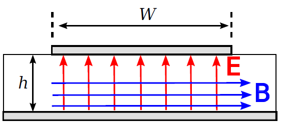
A microstrip line nominally exhibits TEM field structure. This structure is shown in Figure 3.11.2. Note that electric and magnetic fields exist both in the dielectric and in the space above the dielectric, which is typically (but not always) air. This complex field structure makes it difficult to describe microstrip line concisely in terms of the equivalent circuit parameters of the lumped-element model. Instead, expressions for

directly in terms of

and
are typically used instead. A variety of these expressions are in common use, representing different approximations and simplifications. A widely-accepted and broadly-applicable expression is:2

where

and

is

adjusted to account for the thickness

of the microstrip line. Typically

and

, for which

. Simpler approximations for
are also commonly employed in the design and analysis of microstrip lines. These expressions are limited in the range of
for which they are valid, and can usually be shown to be special cases or approximations of Equation 3.11.1. Nevertheless, they are sometimes useful for quick “back of the envelope” calculations.


It turns out that the electromagnetic field structure in the space between the conductors is well-approximated as that of a uniform plane wave in unbounded media having the same permeability

but a different relative permittivity, which we shall assign the symbol

(for “effective relative permittivity”). Then

In other words, the phase propagation constant in a microstrip line can be approximated as the free-space phase propagation

times a correction factor

. Then
may be crudely approximated as follows:

i.e.,
is roughly the average of the relative permittivity of the dielectric slab and the relative permittivity of free space. The assumption employed here is that
is approximately the average of these values because some fraction of the power in the guided wave is in the dielectric, and the rest is above the dielectric. Various approximations are available to improve on this approximation; however, in practice variations in the value of
for the dielectric due to manufacturing processes typically make a more precise estimate irrelevant.
Using this concept, we obtain

where

is the free-space wavelength

. Similarly the phase velocity

, can be estimated using the relationship

i.e., the phase velocity in microstrip is slower than

by a factor of
.
Exercise
50 Ω Microstrip in FR4 printed circuit boards.
FR4 is a low-loss fiberglass epoxy dielectric that is commonly used to make printed circuit boards (see “Additional Reading” at the end of this section). FR4 circuit board material is commonly sold in a slab having thickness

with

. Let us consider how we might implement a microstrip line having

using this material.
Since

and
are fixed, the only parameter remaining to set
is
. A bit of experimentation with Equation 3.11.1 reveals that

yields

for

. Thus,
should be about 3.15 mm. The effective relative permittivity is

so the phase velocity for the wave guided by this line is about

; i.e., 60% of
. Similarly, the wavelength of this wave is about 60% of the free space wavelength.
Footnotes
Additional Reading
- “Microstrip” on Wikipedia.
- “Printed circuit board” on Wikipedia.
- “Stripline” on Wikipedia.
- “Single-ended signaling” on Wikipedia.
- Sec. 8.7 (“Differential Circuits”) in S.W. Ellingson, Radio Systems Engineering, Cambridge Univ. Press, 2016.
Ellingson, Steven W. (2018) Electromagnetics, Vol. 1. Blacksburg, VA: VT Publishing. https://doi.org/10.21061/electromagnetics-vol-1 CC BY-SA 4.0
Explore CircuitBread


Get the latest tools and tutorials, fresh from the toaster.


