What are the basics of a semiconductor?
Published
Before semiconductor devices existed, vacuum tubes were the only devices available for signal amplification, switching, and other applications. Though vacuum tubes are functional, they are bulky, require a high operating voltage, and are inefficient. When semiconductor devices like transistors were invented, semiconductors started to acquire a dominating role in electronics.

Semiconductors are materials that are in between conductors and insulators when it comes to the ability to conduct electrical current, which explains the name. The most commonly used semiconductor material in the electronics industry is silicon. After that, it’s a compound known as gallium arsenide. Though germanium was used extensively in the early years of semiconductor technology, it is unstable at high temperatures, so silicon became more widely used.

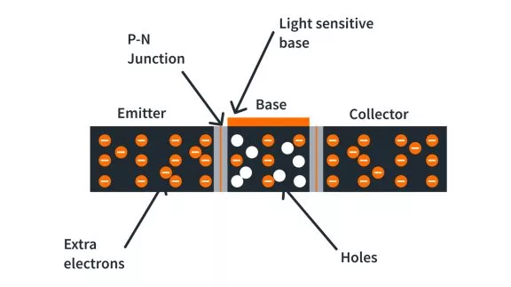
Semiconductor materials have two current carriers, free electrons and holes. In an intrinsic semiconductor material, free electrons are produced when the material receives sufficient thermal energy that provides valence electrons from the valence band enough energy to jump to the conduction band and turn into free electrons. When valence electrons jump to the conduction band, they leave vacancies in the valence band. These vacancies are called holes. The number of holes in the valence band is just equal to the number of free electrons in the conduction band in this undoped, intrinsic material.

A semiconductor material becomes a useful electronic component by controlling its conductivity. However, semiconductor materials, in their intrinsic state, do not conduct current well. This is because of the limited number of free electrons and holes in it. But through a process known as doping, the conductivity of a semiconductor can be increased. Doping increases the number of current carriers by adding impurities with either more free electrons or holes to the intrinsic semiconductor material.

The number of free electrons in an intrinsic semiconductor material is increased in the doping process by adding pentavalent impurity atoms, or atoms with five valence electrons such as arsenic, phosphorus, bismuth, or antimony. For example, an antimony atom covalently bonds with four adjacent silicon atoms during the doping process. Only four valence electrons of the antimony atom were used to form covalent bonds with the silicon atoms, leaving an extra atom that becomes a free electron. So by adding pentavalent impurity atoms to an intrinsic semiconductor material, the number of free electrons can be increased as well as the conductivity of the semiconductor material. Semiconductors doped with pentavalent atoms are n-type semiconductors, since the majority of its current carriers are electrons. Once you add these impurities to an intrinsic semiconductor, it is considered an extrinsic semiconductor.

In order for an intrinsic semiconductor material to have more holes, they are doped with trivalent impurity atoms. These are atoms with three valence electrons in their valence shell like boron, indium, and gallium. For example, when a boron atom covalently bonds with four adjacent silicon atoms, a hole is produced. This is because, each of the four silicon atoms requires one electron from the boron atom, but it only has three valence electrons. In this case, we can say that by adding more trivalent impurity atoms to an intrinsic semiconductor material, it increases the number of holes and improves the conductivity of the semiconductor material. Semiconductors doped with trivalent atoms are p-type semiconductors since the majority of its current carriers are holes.

The doping process converts an intrinsic semiconductor material into extrinsic and produces either an n-type or a p-type semiconductor material. Combining the n-type and p-type semiconductor materials creates a boundary known as p-n junction. This p-n junction is the basis for different semiconductor devices widely used today like diodes, transistors, and thyristors.
In this video, we talked about the basics of semiconductors, the intrinsic semiconductor and its poor conductivity, how doping increases the number of current carriers in a semiconductor material and improves its conductivity. We also briefly mentioned how different semiconductor devices were created based on the p-n junction. If you have any questions, leave it in the comments below and if you’ve found this interesting or helpful, please subscribe to our channel and like this video!
Check Yourself
8 Questions

Get the latest tools and tutorials, fresh from the toaster.


