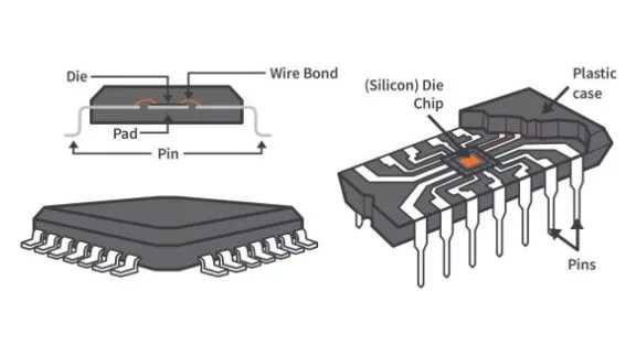
Semiconductors are a fundamental part of modern technology, and today, we will look at one of the basic concepts related to them - energy bands, and how they are formed.
Understanding Energy Bands
Energy bands in semiconductors are essential because they govern the electrical properties of these materials. These bands are formed due to the interplay of overlapping energy levels when atoms come together in a lattice. Let’s understand this in detail now.
Take a sodium atom. It has an atomic number of 11 - hence, 11 electrons are present in its atom. The atomic configuration of the same is shown in Figure 1 below:

This follows the configuration as taught in any basic chemistry course, but let’s review it again. The electron configuration of atoms follows Pauli's exclusion principle, which states, "No two electrons in an atom can have the same quantum states.” An s shell can accommodate two electrons each, while a p shell can accommodate six electrons each. The 1s shell has two electrons in opposite spins. Hence, there are two available quantum states in the 1s shell. Same holds for 2s and 3s. In the 3s shell, since there's only 1 electron, this electron occupies one of the two available quantum states.
The p shell has three different orbitals or subshells, one along each of the x, y, and z axes of 3-D space. There are six electrons in the 2p shell, two opposite spins in each subshell. Hence, there are six different quantum states available in each p shell. Further, the electrons occupy shells in increasing order of energy, as in, first 1s, then 2s, then 2p, and so on.
This was for a single isolated sodium atom. But what does this atomic configuration look like for, say, two sodium atoms taken together?

When two atoms come close together, the 1s energy level splits into two separate sections (represented by two lines in Figure 2) to still respect Pauli's exclusion principle. The immediate observation is doubling of the number of quantum states as they form a combined energy level. (Double because we have two sodium atoms). The electrons from each atom can now occupy the precisely available four quantum states. Let's extrapolate and see what happens in a solid mass of sodium metal. Refer to Figure 3.

Assume the solid mass of sodium metal consists of N atoms(assume N>>1). As you can see in Figure 3, since we have N atoms now, we have N times the quantum states as in an isolated sodium atom. These lines are so close together that they form continuous band-like structures, which are called energy bands.
Further, since the 1s, 2s & 2p shells were completely filled in the atoms, the 1s, 2s, and 2p bands’ quantum states are also completely filled. The 3s orbital in an isolated sodium atom has only one electron, and hence, the 3s band is half-filled with N electrons from N sodium atoms occupying N of the 2N available quantum states. This half-filled band is referred to as the conduction band. The completely filled band present just below the conduction band will be referred to as the valence band. In the Figure 3 above, the 2p band is the valence band.
To solidify our understanding, let's apply what we have learned to magnesium. Magnesium has 12 electrons, and its electronic configuration is shown in Figure 4.

Note that magnesium has two electrons in the 3s shell. Let's see what the band structure of magnesium, a metal, looks like. Look at Figure 5 below.

We can see that 3s band is completely filled as all 2N states are occupied. By definition, the valence band should always be completely filled. Hence, the 3s band now becomes the valence band. What about the conduction band then? The 3p band forms the conduction band contrary to that of the sodium, where the half-filled 3s band forms the conduction band. The conduction band can be either empty or partially filled.
The following observations are accurate for temperature at 0K. At any temperature above that, electrons have thermal energy associated with them, which enables them to have enough energy to move around. Before we get into that in detail, there's one more concept to make note of.
Let's take a closer look at the band structure in sodium metal again. Refer to Figure 6 below.

Note that bands of lower energy are narrower than those of higher energy. This is because the electrons in the lower levels are more tightly bound to the nucleus and, hence, don't move around much. However, the electrons are not as tightly bound at higher levels, so they move in a larger area. In metals especially, the electrons in the outermost shell are held loosely by the nucleus. This leads to an overlap of energy levels in metals. Coming back to sodium, 3s being the conduction band, it still has N quantum states ready to be occupied out of the 2N states that it has. This means that the electrons can move around and occupy any of the remaining N quantum states of the 3s band. This is why sodium is an excellent conductor of electricity. This was for sodium, but what about magnesium, where we have a completely filled valence band?
In metals, as mentioned earlier, the adjacent bands overlap (i.e., there's no band gap). This means the actual band structure in magnesium looks like the one in Figure 7 given below.

The completely filled 3s band and the empty 3p band overlap. The electrons in magnesium’s 3s(valence) band can now move easily to the 3p(conduction) band. So to conclude, metals are characterized by:
- Partially filled conduction band where the remaining quantum states allow for electron movement.
- Completely filled valence band, which overlaps with an empty conduction band, allowing for electron movement and promising excellent conductivity again!
In semiconductors and insulators, however, a proper band gap separates the conduction and valence bands. The same can be seen in Figure 8 below. This region has no energy associated with it and has no electrons in it. The size of the band gap significantly influences the semiconductor's properties and behavior. Let's discuss this in detail now.

Band gap and energy bands in Conductors, semiconductors, and insulators
Take a look at Figure 9 below, which shows the different materials and their band gaps.

We’ve already discussed metals in detail. In insulators, the band gap is substantial. The electrons are confined to the valence band, and none of them can jump to the conduction band due to the very high band gap. This can range as high as 5.5eV. With this very large band gap, even when a large amount of energy is injected into the system, electrons in the valence band cannot break away from the nucleus and enter the conduction band. Due to the lack of electrons in the conduction band, meaning there are no electrons that can move freely, insulators do not allow electricity to pass through them.
Then comes the semiconductor, which lies between the two extremes. Refer to Figure 10 below.

The band gap of these materials is around 1-1.5eVs, which, at room temperature, allows valence electrons to have sufficient energy to move into the conduction band. When electrons move from the valence band to the conduction band, they leave a hole behind in the valence band. Both the electrons in the conduction band and the holes in the valence band serve as charge carriers. The holes do so by permitting a certain freedom of movement to the electrons remaining in the valence band, electrons that, in the absence of holes, would be gridlocked. The conductivity can further be manipulated by doping, that is, changing the material's chemical makeup and modifying the range of the different bands. In this way, we can control the semiconductor material’s conductivity.
Doping: Altering band structure of the semiconductor material
Doping is adding impurities to the silicon material to alter the number of electrons to control its conduction. If you read the previous tutorials on semiconductors, you’ll know that there are two types of doping and, hence, two types of semiconductors: N-type and P-type.
In n-type doping, additional electrons are introduced into the material by adding an impurity with more electrons than the dominant atom used (typically silicon). These electrons increase the electron population in the conduction band and enhance its conductivity. Conversely, p-type doping creates holes in the valence band by introducing atoms with fewer electrons in the conduction band than silicon. Electrons from the neighboring atoms jump into the holes in the lattice, leaving behind a hole in their parent atom. This movement of holes in the valence band effectively contributes to the conduction of electricity in the p-type semiconductors.
In the PN junction, valence band alignment allows hole movement from P-type to N-type, while conduction band alignment facilitates electron movement from N-type to P-type. The depletion region, caused by migrated charges, establishes a barrier potential. Forward bias reduces the barrier, allowing current flow, while reverse bias increases it, inhibiting current flow. This is discussed more in-depth in our tutorial dedicated to PN junctions.
Energy bands are building blocks that control the semiconductor behavior, laying the foundation for the design of modern-day electronic devices. The energy bands and their effect on the PN junction are central to semiconductor technology.
