In this FAQ, we will be learning about the simplest type of field effect transistor (FET) - the Junction Field Effect Transistor (JFET). JFETs, like other FETs, are semiconductor devices. They are used in amplifiers, embedded systems and in communication circuits as switches and amplifiers.
Before we begin to learn about JFET, it might be beneficial to review the basics of semiconductors. From this link, you can find several detailed tutorials dealing with semiconductor physics from the most basic principles.
Basics of FETs
In all FETs, the path of flow of the charge carriers in the device is known as the channel. If the channel is made up of an n-type semiconductor material, it's known as an n-channel FET. Similarly, a p-channel FET’s channel material is of p-type semiconductor. Look at the image 1 below:
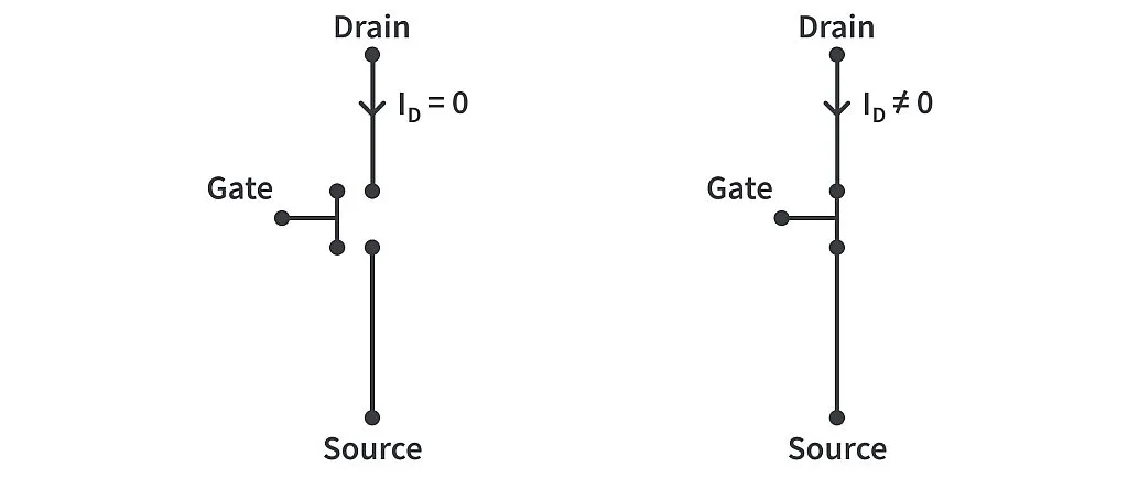
The image shows the generalized symbol of FETs. The current flow in FETs happens between two terminals on the device – the source and the drain. The current flow is controlled by applying a voltage at a third terminal – the gate. This voltage creates an electric field across the device that affects and controls the current flow – hence the name “field effect transistors”. Depending on the kind of voltage we apply at the gate which may be used either to turn on or turn off the device, we have different kinds of FETs.
Fabrication of the JFET and its structure
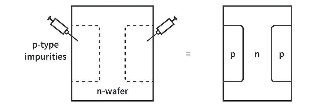
To fabricate a JFET, first, the manufacturer takes an n type semiconductor wafer. This will form the base semiconductor wafer, or the substrate, as more commonly known in semiconductor technology.
Specific regions on either side of this n type substrate are now converted to p-type by doping p-type impurities to the specific area of the substrate as shown in Image 2.
Before understanding why this is done in a JFET, it's beneficial to first review what happens when a p-type and n-type semiconductor meet each other side by side. A brief discussion of the same is given in the next section, but it's highly recommended that you can refer to the tutorials linked to get a better grasp of the subject.
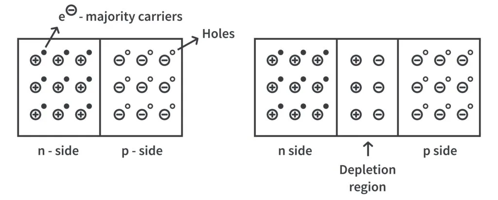
Both n- and p-type semiconductors have mobile charge carriers – electrons and holes respectively. Referencing image 3 below, you can see that when a p-type semiconductor meets an n-type semiconductor, the electrons from the n side move to the p side and combine with the holes there. As they do so, they leave behind positive fixed ions on the n side. Negative fixed ions are similarly formed on the p side when the hole and the electron combine. This side-by-side region of immobile positive and negative ions is known as the depletion region – a region depleted of mobile charge carriers. The width of the depletion region can be increased by reverse biasing the pn junction.
As p wells are formed in the n substrate of the JFET, a pn depletion junction is formed along the boundary where the p well meets the n substrate. As you can see in image 4 below, the n-channel is flanked by the two depletion regions on either side. This is the internal construction of the JFET. Metallic contacts are provided at the drain and the source and on either side of the substrate where the two p wells are. The contacts of the p wells are tied together into a third terminal – the gate. The n-channel JFET is now ready for use. To operate the device, a positive voltage VDD is applied between the drain and the source. Electrons will begin to flow from the source to the drain. The conventional current here is from drain to source.

Channel pinch off in JFETs
Apart from the current flow, there is one other important thing happening inside the JFET. Look at image 5 below and see that the n-channel is like a spread-out resistor. And as current passes through the channel, there is a voltage drop across the channel. You can see the image below where, for example, VDD has been taken as 5V and VGS as 0V. The positive voltage because of VDD in the n-channel and the p wells at ground potential will reverse bias the pn junction.
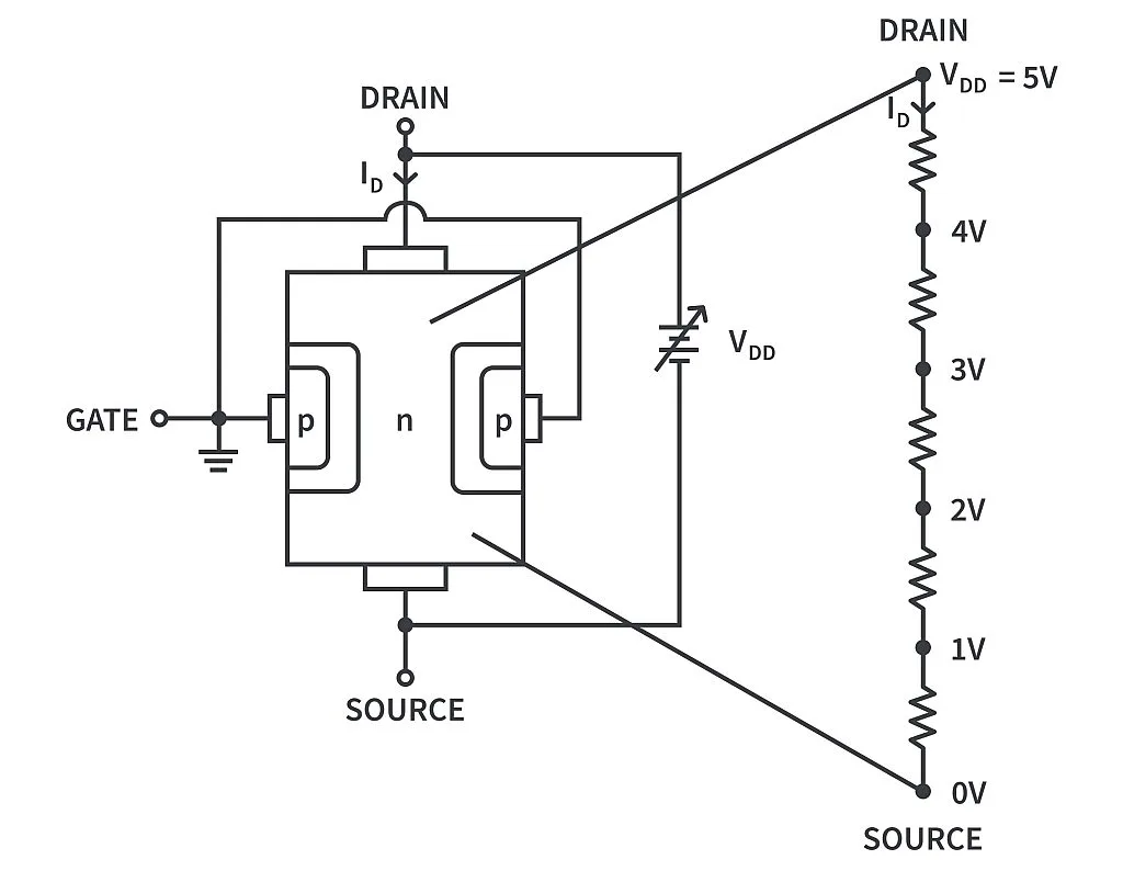
As the absolute voltage at the top of the channel is more than that at the bottom of the channel, the depletion region width is not uniform and takes a form as shown in image 6 below.
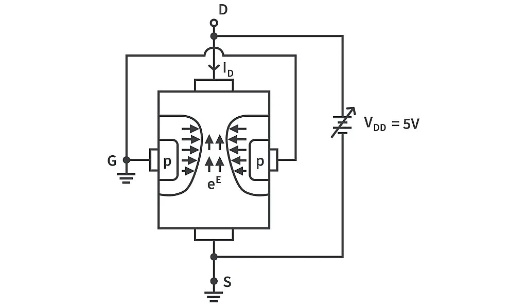
What happens if you keep increasing VDS? The current will increase and so will the width of the depletion region (especially at the top near to the drain) as it gets more and more reverse biased. Soon there will be a point where the depletion regions from either side of the channel expand inwards and touch each other until there is hardly any channel left in between. This is known as the channel pinch off and the voltage VDD ( = VDS ) at which this occurs is known as the pinch off voltage.
As we increase the voltage VDS further, the depletion regions do approach each other at the top, and at VP they come very close to each other. But if they end up touching each other, there is no n-channel left for the drain current to flow. And as soon as ID goes to 0, there is no voltage drop across the channel which was causing the reverse bias of the channel and p wells in the first place. Thus, there is a narrow strip of n-channel between the two-depletion regions where ID can flow. However, the depletion regions can be made to touch each other deliberately, thus sending ID to 0. This is, in fact, the turn off process (forcing ID → 0) of the JFET which we will discuss later.
I-V characteristics of JFET
A graph of ID vs VDS (the output characteristic of JFET) is shown in image 7 below. Until VP the pinch off voltage, current increases linearly. As the voltage nears the pinch off voltage, the current increases and so does the resistance of the channel to the current flow. This is obvious since the channel width available for current flow is decreasing as the depletion regions from each side expand more and more into the channel. After the pinch off voltage, the current can increase no more and becomes saturated at IDSS. The curve here is flat and the channel resistance is very high.
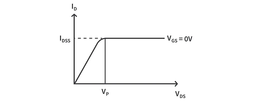
Note that the curve in image 7 is plotted for a gate voltage of VGS = 0V. A JFET is a ‘normally on’ device. Decreasing VGS from 0 can cause the actual pinch off of the channels to occur much sooner (and sending ID to 0) as shown in image 8 below.
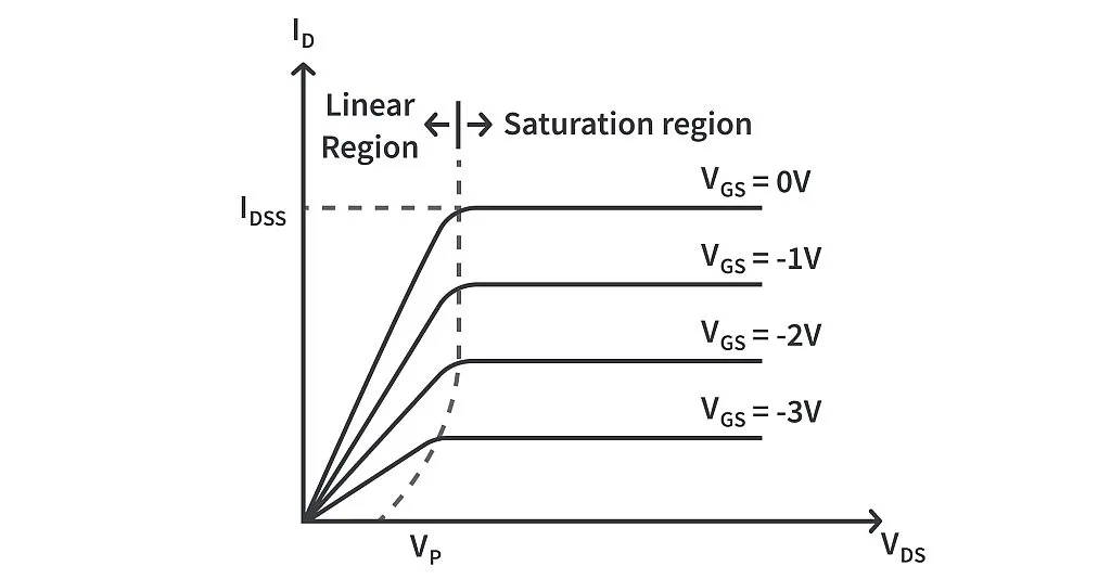
This is because a negative VGS reverse biases the pn junction more easily than with VGS = 0V. Therefore, by applying a negative voltage at the gate, the device can be turned off. Such devices where a voltage must be applied to the gate to turn OFF the already ON device are known as depletion mode devices – and JFET is one of them. Contrarily, the MOSFET is an enhancement mode device where a voltage at the gate is used to turn ON the device.
For the JFET, the region where the channel current is linear to the voltage VDD is known as the linear or ohmic region. And the region where the current is constant irrespective of VDS is the saturation region. JFET operating in this saturation region behaves as a constant current source - this is one of the common applications of a JFET.
p-channel JFET
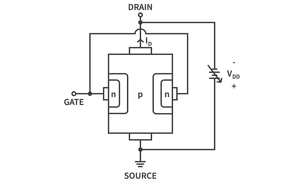
Thus far, we have been discussing the n-channel JFET. On the other hand, the p-channel JFET is shown in image 9. The substrate is p-type hence the name p-channel JFET. Two n wells are made at either side of the substrate.
When we talk about the source and drain terminals in a JFET they may seem interchangeable as they look symmetrical from the images, but there are minute differences between the two terminals at the semiconductor level which are a part of the fabrication process. While the source is always kept at ground, the drain is kept at a positive potential for an n-channel JFET and kept at negative potential for p-channel JFET. In the p-channel JFET, a positive voltage is applied at the gate to turn off the device.
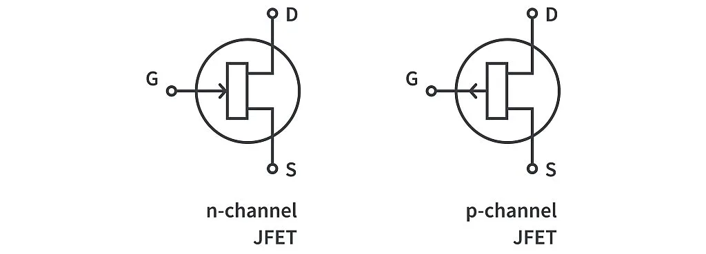
The symbols for both the JFETs and their notations are given in the image 10 below.
JFET is the simplest type of the FETs. They offer high input impedance on the order of 1012 Ω. The input current to the gate is on the order of a few pico-amperes. However, MOSFETs have far surpassed the applications and uses of JFETs. Mostly this is due to the fact that the voltages applied both to the gate and drain of the MOSFET are the same polarity- either both positive or both negative. Even so, they are less prone to noise and the absence of oxide layer makes them more “rugged” compared to that of MOSFET, securing their place in circuits of special applications.
