Write a Hello World Program | Embedded C Programming - Part 2
Published
Hello again! In the previous tutorial I told you about the PIC18F14K50 MCU and the required hardware and software tools to work with it. Today, we’ll assemble a simple circuit and write our first traditional “Blink” program that will flash an LED connected to a pin of the microcontroller.
Without a long introduction, let’s consider the schematics diagram that will implement the given task (Fig. 1).

As you can see, the PIC18F14K50 MCU looks monstrous in comparison to our simple and cozy PIC10F200. Let’s try to figure out what’s written here. Almost every pin of this MCU except for the power pins VDD, VSS, and VUSB, has several functions. I’d better copy the table from the data sheet of this microcontroller (which can be found on this page: https://www.microchip.com/en-us/product/PIC18F14K50#document-table) which will explain the pins’ functions better (Table 1).
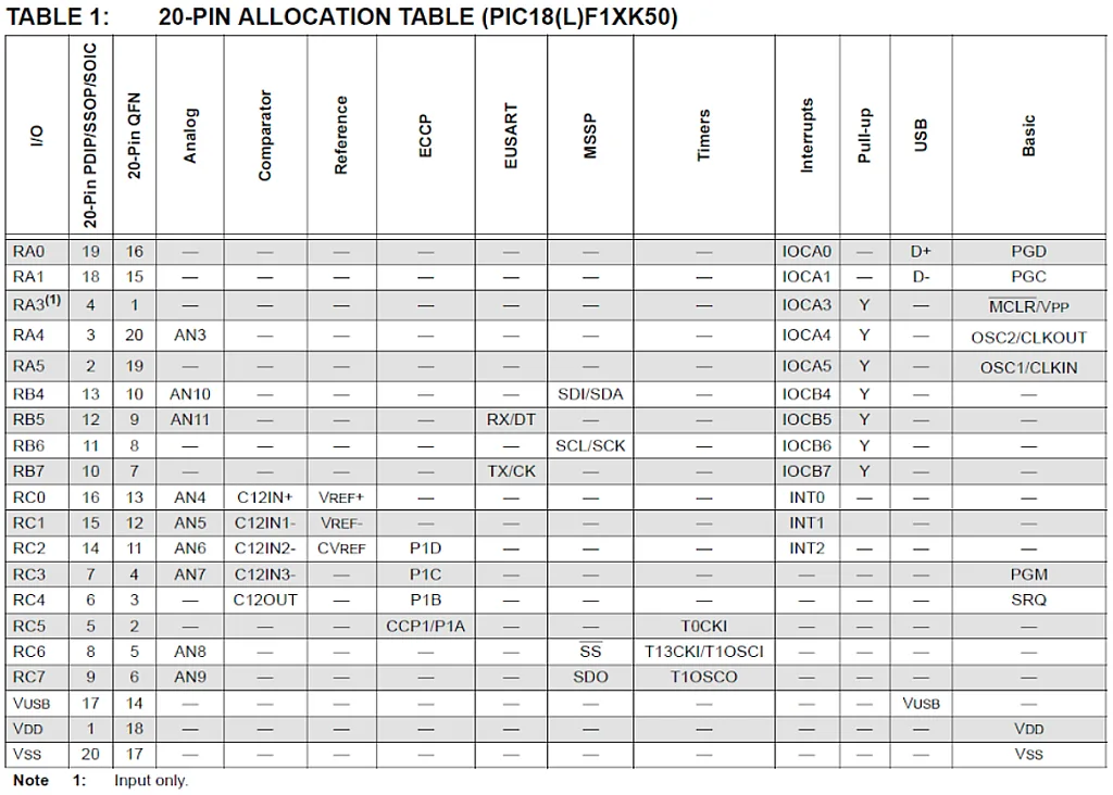
In Table 1 you can see the modules names in the upper row and the functions which pins implement for the corresponding modules inside the table. We will return to this table when we consider these modules, and for now we only need the first and second columns. Unlike the PIC10F200, where general purpose I/O pins were called just GP0, GP1 etc., this MCU has three independent I/O ports named RA, RB, and RC. Each port has up to eight I/Os with numbers from 0 to 7. Thus RA0 is pin #0 of the RA port, and so on.
As you can see from fig. 1, we connected LED1 through the current-limiting resistor R1 to the RC0 pin. The connection to the PICKit debugger remains the same: VPP for high programming voltage, VDD for positive power, VSS for negative power, PGD and PGC for programming data and clock correspondingly.
Now, as we have dealt with the connection, let’s open MPLAB X and create the firmware to blink the LED. I’ve already talked how to create a new project in one of the PIC10F200 tutorials (https://www.circuitbread.com/tutorials/circuit-setup-mplab-x-ide-part-4-simple-microcontroller-pic10f200) but it won’t hurt to repeat this again, moreover there are some differences. So to create the new project you need to select “File” - “New Project…” in the main menu, then you will see the following window (Fig. 2)

Here we select “Standalone project” in the right part and click “Next” (Fig. 3).

In this page we need to select the correct device “PIC18F14K50” (or whichever you use), also optionally you can select the Tool. As I mentioned in the previous tutorial, I prefer the PICKit3, so I’ll select it, but you need to select the one you have. Then click “Next” (Fig. 4).

For now, we are not going to perform any debugging so we select “None” in the drop-down list. We can always change our choice later in the project properties. Then click “Next” (Fig. 5).

For some reason the “Select Plugin Board” step was skipped, and we get to the compiler selection page. As we’re going to use the C language, we need to select XC8. In my case I have two versions installed, and I will select the latest one. You will probably have only one version, so please select it and click “Next” (Fig. 6).

In this page you need to select the project name (I used “Blink”) and project folder (you can select whatever is more convenient to you), also select “Use project location as project folder” to have all project files in one place. As for Encoding, frankly, I’ve never changed it and always leave it the default value. Now our project is ready to be created, so we click “Finish” and return to the main screen. There you can see the project summary in the left bottom “Dashboard” part.
As you can see, the project is empty, and has only a Makefile file. So we need to right click on the Source Files folder, then select “New” and then “main.c…” (Fig. 7)

You will see the following window (Fig. 8).

I selected the name “main” and extension “c” as this is the common practice in C language to call the main file of the application (and in our case, the only source file) “main.c”. Then you may click “Finish” and return to the main screen again. Now we have the file in which we will write our code. It already has some lines (Fig. 9).

In this file we will write the following code:
#define _XTAL_FREQ 1000000  //CPU clock frequency

#include <xc.h>         	//Include general header file

void main(void)         	//Main function of the program
{
	TRISCbits.TRISC0 = 0;   //Configure RC0 pin as output
	while (1)           	//Main loop of the program
	{
  	    LATCbits.LATC0 ^= 0x01;//Toggle RC0 pin
  	    __delay_ms(500);  	//500ms delay
	}
}
In my explanation of the code I will consider that you are at least superficially familiar with the C language. Otherwise, please read some book or tutorial about it, as these tutorials are about microcontroller programming but not C language basics. If you have any programming experience, there shouldn’t be anything too surprising in the syntax.
In line 1 we define _XTAL_FREQ macro as 1000000. This macro should be named exactly this, as it’s used in delay functions. Its value represents the CPU frequency in Hertz. By default the frequency of the internal oscillator is 1 MHz so we write this value here.
In line 3 we include the “xc.h” file into our project. As you remember from fig. 9 this line was generated automatically. You should leave it, as it consists of the other includes and definitions that allow us to use the normal names of the registers and bits of the MCU.
In line 5 the main function of the program starts. As you know, it’s always called “main”. In our case it doesn't accept or return any values, that’s why we write “void main (void)”.
Line 7 also should be vaguely familiar to you if you read the PIC10F200 series. As you remember the TRIS operator was used to change the pin direction - input or output. Here it is almost the same but unlike the PIC10F200 MCU, PIC18F14K50 (and actually the majority of others) has the TRIS register for each of available I/O ports. In our case we have TRISA, TRISB, and TRISC register. The use of this register is the same as in PIC10F200:
if a bit of this register is set to 1, then the corresponding I/O pin is configured as an input; if a bit is reset to 0 then the corresponding pin is an output.
So, in line 7 we reset bit 0 of the register TRISC, and thus configure pin RC0 as output.
Let’s consider the syntax of line 7 in more detail as this format is used frequently:
TRISCbits.TRISC0 = 0;
The beginning of the sentence is the name of the register (TRISC) then the suffix “bits” is added. This suffix means that we want to operate with one specific bit of this register. The name of this bit is written after the dot. In our case it’s TRISC0 because we want to change bit 0. Actually, TRISCbits is a union in which each bit has its own name TRISCx or RCx (where x is the bit number and changes from 0 to 7). It is defined in the MCU specific header file in the following way:
typedef union {
	   struct {
       unsigned TRISC0             	:1;
       unsigned TRISC1             	:1;
       unsigned TRISC2             	:1;
       unsigned TRISC3             	:1;
       unsigned TRISC4             	:1;
       unsigned TRISC5             	:1;
       unsigned TRISC6             	:1;
       unsigned TRISC7             	:1;
	   };
	   struct {
       unsigned RC0                	:1;
       unsigned RC1                	:1;
       unsigned RC2                	:1;
       unsigned RC3                	:1;
       unsigned RC4                	:1;
       unsigned RC5                	:1;
       unsigned RC6                	:1;
       unsigned RC7                	:1;
	   };
} TRISCbits_t;
So TRISCbits.RC0 is equal to TRISCbits.TRISC0, and you can choose whichever you like.
If you want to operate with several bits of the register, it’s better to use the register name without the “bits” suffix. So the line TRISC &= ~0x01 will also be equal to TRISCbits.TRISC0 = 0. Let’s go into why that is.
Operation “&=” means bitwise AND with the operand. And operation “~” means the bitwise inversion of the operand. So “~0x01” will invert the 0x01 value:
0x01 = 0b00000001
~0x01 = 0b11111110 = 0xFE
After that, the AND operation will be performed between the contents of TRISC and the 0xFE value. I think I already explained in the PIC10F200 series that this will lead to resetting only bit 0 of the register while other bits will remain unchanged. This is a very common practice when setting or clearing bits in a register.
The variant TRISC &= ~0x01 is obviously more difficult to understand than TRISCbits.TRISC0 = 0 from an intuitive perspective but when you need to change some bits at once, this can be more beneficial. Compare:
TRISC &= ~0x55	    and		TRISCbits.TRISC0 = 0;
					        TRISCbits.TRISC2 = 0;
					        TRISCbits.TRISC4 = 0;
					        TRISCbits.TRISC6 = 0;
On the other hand, using the register name with the “bits” suffix will help you not to make a mistake by showing which bits are available. For instance port RB has only four pins: RB4-RB7, so only TRISB4 - TRISB7 are available in the TRISBbits union.
OK, now that we are aware of how the register names are formed, it will be easier to understand the next lines.
In line 8, the endless loop starts. The “while” loop is active while its argument is true. And as 1 is always considered as “true” we will never leave the while loop and will implement the lines 10 and 11 forever as long as power is applied to the MCU. We used a similar approach with the PIC10F200 using Assembly as well, but there we made this by means of the GOTO operator.
In line 10, we have a sentence similar to line 7 by syntax:
LATCbits.LATC0 ^= 0x01;
Now we know that the LATC is the name of a register, and LATC0 is the name of a bit. Operation “^=” implements the XOR function between the bit LATC0 and the value 0x01. As you probably remember from the PIC10F200 tutorials the XOR function changes the corresponding bit to the opposite state. So the sentence LATCbits.LATC0 ^= 0x01 will toggle the bit LATC0 of the LATC register between 1 and 0 at every iteration of the main loop.
Let’s consider the meaning of the LATC register. It is the port data latch register (LATch). This means that writing 1 into a bit of this register sets the corresponding pin high, and writing 0 sets the pin low (of course, the pin should be configured earlier as an output). Like the TRISx registers, there are LATx registers for each IO port: LATA, LATB, and LATC.
As a bonus, let’s also consider the last register that every I/O port has. It’s called PORTx, and thus there are PORTA, PORTB, and PORTC for the corresponding I/O port. This register, when read, consists of the real state of each I/O pin. So, for instance, reading the PORTCbits.RC0 will contain the current state of the RC0 pin. If it’s 1, then the pin is high, if it’s 0 then the pin is low. You can also write to this register, and the result will be the same as with writing to the LATx register. Literally, the same.
Actually, you also can read the LATx register, and it will contain the port latch state: 1 for high, 0 for low. So what’s the difference between these two registers, and why do we need both if they seem to do the same?
The difference is in the read value. The PORTx register reads the actual state of the pin while LATx reads the state of the output latch. The difference may seem insignificant but it exists. Let’s consider the following situation: We change the pin state from low to high by writing 1 into the LATx or PORTx register (at the moment, there really is no difference between these). Right after that we read the LATx and PORTx value. The LATx value will definitely be 1, because we have written 1 there right now. But with the PORTx register the result may be undefined because the real state of the pin may still be low because the voltage still hasn't risen enough, or it can be already high - we won’t know until we read it.
So in operations of read-modify-write type (like we have in line 10) Microchip recommends using the LATx register to be sure we read the value that we had written there before.
Now, let’s consider the line 11:
__delay_ms(500);
The name of the function seems to be quite clear. It performs the delay for the specified amount of milliseconds, in our case the delay is 500 ms. There is also a similar function __delay_us() which performs the delay in microseconds. For proper operation of these functions you need to specify the correct CPU frequency in the _XTAL_FREQ macro.
Nobody is preventing you from making a manual delay function like we did with PIC10F200 MCU, by implementing the loop with a big number of iterations, but why would you? Here we have a convenient function that provides us a code size-optimized and precise delay.
OK, we’ve gone over the whole code, and now we can assemble the circuit according to the schematic diagram (fig. 1) and connect the PICKit to the PC.
Then we need to Build the project by clicking on the hammer icon or using the “Production-Build project (Blink)” menu point. If there are no issues, you will see the notification “BUILD SUCCESSFUL (total time: 1s)” in the “Output” window (Fig. 10)

Also in the “Blink-Dashboard” window you can see the project statistics. The data memory usage is just one byte, and the program memory usage is 38 bytes. For comparison, the same program in Assembly language spent 2 bytes of data memory and 17 bytes of program memory (https://www.circuitbread.com/tutorials/how-to-blink-an-led-part-6-microcontroller-basics-pic10f200). That’s kind of the status quo going from C to Assembly: Flash consumption doubled while RAM consumption halved.
Now let’s set up the debugger. To do this, select “File - Project Properties (Blink)” in the main menu. In the left part of the window select “PICKit 3” (or “PICKit 4” if you use it). You will see the following tab (Fig. 11).

In the “Option categories” drop-down list select the “Power” line (Fig. 12)

Check the box “Power target circuit from PICKit3”, also select the voltage level. Be attentive, if you have the PIC18LF14K50 or PIC18LK13K50 MCU, you need to set the voltage lower than 3.6 V (for instance 3.25V or 3.5V). For other MCUs you can freely set up to 5.0V. When you are done with these settings, click OK.
Now we are good to go. Press the green triangle icon “Run Project (Blink)”. You will have a warning (Fig. 13)

It’s the same warning that I told you about in the previous paragraph. Click “OK” and wait while the project is being downloaded.
If you have an error like this:
"PICkit 3 is trying to supply 5.000000 volts from the USB port, but the target VDD is measured to be 4.750000 volts. This could be due to the USB port power capabilities or the target circuitry affecting the measured VDD.The target circuit may require more power than the debug tool can provide. An external power supply might be necessary.Connection Failed"then try to reduce the supply voltage to 4.5 V.
Finally, you should see the “Programming/Verify complete” notification. And… nothing! The LED doesn’t blink at all. What’s the problem with it?
Well, first, calm down, it’s not your fault. For some reason (and I really don’t understand why it’s done in such a stupid weird way) the clock source is initially set as “External RC Oscillator”, which means that you need to connect an RC-circuit to the OSC1 pin of the MCU to provide a clock to the MCU. The PIC18F14K50 has an internal oscillator also which can provide the frequency from 31 kHz to 16 MHz (the default value is 1 MHz), and I don’t know why it’s not selected as a default option.
To use the internal oscillator we need to set and write the correct values of the configuration bits. I think you remember that we did the same with the PIC10F200 MCU (__CONFIG _WDT_OFF & _CP_OFF & _MCLRE_OFF). But that MCU had just one configuration register, while the PIC18F14K50 has twelve(!!!) configuration registers. I will talk about each of them as we need them. And for now we will set the correct clock source.
To change the configuration bits, you need to select “Production - Set Configuration Bits” in the main menu. You will see the following window in the right bottom part (Fig. 14)

Here you need to change the three values which are marked with red frames in fig. 14. Changing them is very simple, you just need to click on the value and select the proper one in the drop-down list (Fig. 15)

The FOSC value sets the clock source, and we need to select “Internal RC oscillator” here. Also, we need to disable the watchdog timer (as we did with PIC10F200) by changing the WDTEN value to “OFF”. And finally we need to disable the Low-voltage programming interface by setting the LVP value to “OFF” (I really don’t know why this is required but for me, the LED blinked very quickly regardless of the clock settings until I disabled the LVP).
Now we need to transfer the configuration bits settings to our program. To do this, set the cursor at the first line of the code, and then right click on the configuration bits, and select the “Insert Source Code in Editor” in the drop-down menu (Fig. 16)

After that, all the configuration bits will be transferred to your code, and the program will become much larger. For some reason it also creates the line “#include <xc.h>” which we already have, so you can delete the spare one (Fig. 17).

Now let’s try to run the project again. This time everything should be good, and you finally see the LED blinking with the frequency of 1 Hz. And if it’s not, then try to find the mistake in your code, configuration, or settings.
And that’s finally it for now. I really didn’t expect this first tutorial to be so long, but it turned out that a lot of things needed to be explained. In this tutorial we got acquainted with the PIC18F14K50 MCU, created the first project in MPLAB X, and wrote the first program in C language. Also, we got familiar with the TRISx, LATx, and PORTx registers that are used to work with the I/O ports. And finally we figured out that everything is not that simple and obvious with the configuration bits in the PIC18F14K50 MCU.
As homework, try to flash two LEDs in the antiphase, so when one LED is on, the other is off, and vice versa.

Authored By
Sergey Sokol
I was born, raised, and currently live in Ukraine. I’m fond of different types of electronics and backpacking but these things have been set aside with the war that has been thrust on my country, my people, and my family. Through these trials, if you could help support me financially, I would appreciate any help that could be sent via Paypal to sokolsp@gmail.com

Related Tutorials

Related EE FAQs
 work?")
How do Analog to Digital Converters (ADCs) work?

Answered by Uma Bharathi D

What's the difference between a regular relay and a power relay?

Answered by Jayesh Upadhyay

What is a PWM signal?
Answered by Jayesh Upadhyay

Why is RAM faster than other memories?
Answered by Jayesh Upadhyay
Explore CircuitBread
- 244 Tutorials
- 9 Textbooks
- 12 Study Guides
- 31 Tools
- 104 EE FAQs
- 295 Equations Library
- 213 Reference Materials
- 97 Glossary of Terms
Friends of CircuitBread
-

Free Industry Lead Time Monitor
-

Free Electronics Lessons & Resources + 2 Perks
-

Check Out Our Free Ohm's Law Calculator


Get the latest tools and tutorials, fresh from the toaster.


