Signal Generator using 12-bit DAC and Chain Mode of DTC | Renesas RA - 17
Published
Hello again! Today we will keep discovering the digital to analog convertors of the RA2A1 MCU. As I already mentioned in the previous tutorial using the 8-bit DAC there are two types of the DAC modules in it - 8-bit DAC called DAC8, and 12-bit DAC called DAC12 or just DAC.
In this part we will extend the previous task and program: create a two channel signal generator (first channel with DAC8, second channel with DAC12) which will independently produce sine, saw, triangle or trapezoid waves with the same frequency. The waveform and the frequency will be also set via the SEGGER RTT protocol. Like last time, the generation also shouldn’t involve the CPU.
Before switching to the program code, let’s briefly consider the DAC12 module.
Introduction into 12-bit Digital to Analog Converter (DAC12)
The DAC12 module is very similar to DAC8 but has some differences in addition to the resolution.
The output voltage for DAC12 is calculated as:
Here DADR0 is the value written into the eponymous register. As you see, here I wrote its name without “n” at the end. This is because DAC12 has only one channel. Also, here I used VREF instead of AVCC0. This is because the reference voltage for DAC12 is selected from two pairs: AVCC0-AVSS0, and VREFH-VREFL applied to the dedicated MCU pins.
If VREF is greater than 2.7V the conversion time is 1us which gives the max theoretical update frequency as 1MHz. If VREF is lower than 2.7V, you (like with DAC8) need to enable the charge pump generator at the output, and the conversion time in this case also increases but not as drastically as for DAC8 - just up to 1.2 us.
Like with DAC8, the DA conversion can be synchronized with the AD conversion to reduce the noise during the conversion.
The output of the DAC12 can be applied to the output MCU pin, to the built-in operational amplifier (channel 0), or be used as the reference voltage for the only high-speed comparator.
The DA conversion also can be started by the signal from the ELC module to reduce the power consumption and exclude the CPU from this process.
And that’s all about the DAC12 module. If you want to know more about it, you can refer to the RA2A1 user’s manual.
Algorithm of the Operation of the Signal Generator
All other modules that will be used in this part are already familiar to us, so we can consider the algorithm of operation of the project.
In comparison to the previous part, the block diagram of the signal generator became even more complex (Figure 1).
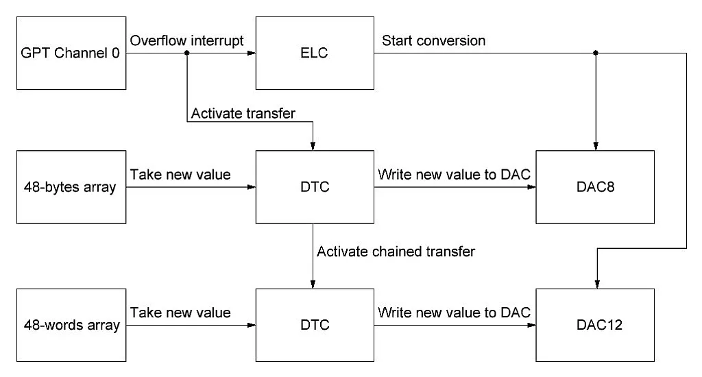
I will not describe the whole block diagram again, you can read about it in the first part. Only the third line has been added here, so let’s consider it in detail.
In the current project there will be two DTC transfers configured - the first one is the same as in the previous part which takes the value from the 48 bytes array and sends it to the DACS0 register of DAC8 module. But this time it will be additionally configured in chain mode. There are two options when using it:
- The next transfer in the chain starts after each previous transfer in the chain.
- The next transfer in the chain starts after the last previous transfer in the chain.
In our case we apparently need to use the first option, as we need to update the DAC12 value every time the DAC8 is updated.
DAC12 starts the conversion simultaneously with DAC8 using the same GPT0 overflow signal which triggers the corresponding ELC event.
Also you can see in Figure 1 that this time there is an additional array of 48 words (here, word means 16-bit value) in which the 12-bit values for the DAC12 module are stored. The calculations of the 12-bit values are the same as 8-bit, you just consider the maximum value as 4095 instead of 255. For example the sine wave formula for DAC12 will be the following:
Where
This is all about the algorithm, let’s now see how it’s all done in the real program.
Project Creation and Configuration
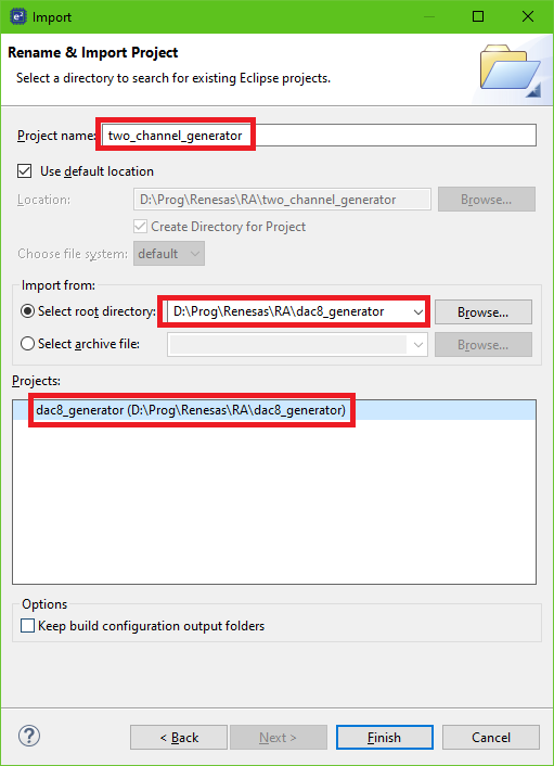
Let’s open e2 studio and perform the “Import” - “Rename & Import Existing/C++ Project into Workspace” action. I have explained in detail how to do this in the second part of tutorial 10. Now we need to make a new project based on the previous one. That time I called it “dac8_generator”, so my “Rename & Import Project” window looks as follows (Figure 2).
Now we can press the “Finish” button and open the “configuration.xml” file of the “two_channel_generator” project. Then switch to the “Pins” tab to configure the output of DAC12. We need to scroll down the “Pin selection” list, find and expand the “Analog:DAC” sublist and select the line “DAC0” which corresponds to the only channel 0 of the DAC12 module. Here we only need to change the “Operation mode” from “Disabled” to “Enabled” and see that the “DA” value now has become “P500” (Figure 3).

There is nothing more to be done here, so we can switch to the “Stacks” tab to add and configure the required stacks. From the previous project we already have the “g_ioport I/O Port (r_ioport)”, “g_timer0 Timer, General PWM (r_gpt)”, “g_elc Event Link Controller (r_elc)”, “g_transfer0 Transfer (r_dtc) GPT0 COUNTER OVERFLOW”, and “g_dac8_0 DAC8 (r_dac8)” (Figure 4).

As follows from the block diagram (Figure 1) we need to add the DAC12 and one more DTC stack. We don’t need to add another ELC stack though because, as I mentioned in one of the previous tutorials, if you add the ELC stack once, you enable the operation of the ELC throughout the whole project. With DTC there is a different situation - you need to add a separate stack for each transfer.
We don’t need to change any properties of the existing stacks, so let’s now add and configure two new ones. Let’s start with DTC. The configuration of the new DTC stack should be as follows (Figure 5).
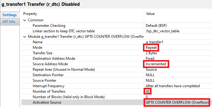
You can see that the configuration of this stack is very similar to the configuration of the first DTC stack (see the first part of this tutorial). There just two differences - the “Name” for this DTC stack is “g_transfer1”, and the “Transfer Size” remains by default as “2 Bytes” because this time we will need to transfer 16-bit value at once into the DADR0 register of the DAC12 module. The same as previous time, we will configure the source and destination pointers in the program code. Also the “Activation Source” for this transfer should be the same as for the previous one - “GPT0 COUNTER OVERFLOW (Overflow)”. For some reason you can’t configure the chain mode in the visual FSP configurator, so we also will do this manually in the program.
Now let’s add the DAC12 stack. To do this we need to press the “New Stack >” button, expand the “Analog” list and select the “DAC (r_dac)” line (Figure 6).
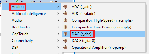
After that the “g_dac0 DAC (r_dac)” block will appear, which we need to configure according to Figure 7.
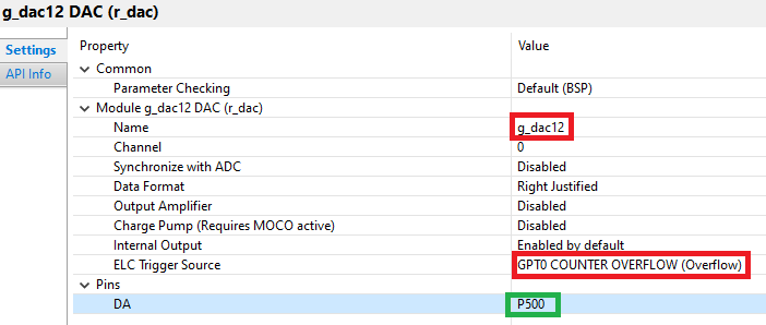
As you can see, the DAC stack also has few parameters like DAC8:
- “Name” is the name of this stack in the program. Let’s change it to “g_dac12” to indicate to ourselves that this is a 12-bit DAC.
- “Channel” selects the DAC12 physical channel. As there is only one channel available, we leave this parameter unchanged.
- “Synchronize with ADC” allows synchronization of the AD and DA conversions to reduce the noise. In our case we don’t use the ADC module, so we can leave this parameter as “Disabled”.
- “Data Format” allows selecting between the “Right Justified” and “Left Justified” bits adjustment. This option specifies whether the 12 bits of DAC value will be the lower or the higher ones in the 16-bit word, respectively. In our case we will use the first option.
- “Output Amplifier” enables the amplifier at the output of the DAC (not applicable for RA2A1 group).
- “Charge Pump (Requires MOCO active)” enables or disables the charge pump at the DAC8 output. As in our case the reference voltage (AVCC0) is greater than 2.7V we can disable it to decrease the conversion time.
- “Internal Output” enables the DAC output to the internal modules like OpAmp or analog comparator. This field has the only value “Enabled by default”.
- “ELC Trigger Source” selects the event which starts the DA conversion. We have agreed (see Figure 1) that we will use the GPT overflow event as a trigger, so we need to find and select the “GPT0 COUNTER OVERFLOW (Overflow)” event.
Make sure that the “DA” pin is set as “P500”.
Here is all about the configuration of the DAC12 module. As usual, for more information about it please refer to the FSP documentation.
After all the configurations, your Stacks Configuration should look like in Figure 8.

Also, let’s switch to the “Event Links” tab and make sure that in the “Allocation” table the DAC80 and DAC120 functions are both linked to the “GPT0 COUNTER OVERFLOW (Overflow)” event (Figure 9).

We have configured everything we need, so now we can click the “Generate Project Content” button and switch to writing code.
Program Code of the Project
We already have all required RTT files added, so now can just open the “hal_entry.c” file and write the program code. In the code below I have highlighted the new lines with the green color.
#include "hal_data.h"
#include "SEGGER_RTT.h"
#include <stdlib.h>

FSP_CPP_HEADER
void R_BSP_WarmStart(bsp_warm_start_event_t event);
FSP_CPP_FOOTER

uint8_t sine_array_8b[48] = {128, 144, 160, 176, 191, 205, 218, 229, 238, 245, 251, 254, 255, 254, 251, 245,
238, 229, 218, 205, 191, 176, 160, 144, 128, 111,  95,  79,  64,  50,  37,  26,
17,  10,   4,   1,   0,   1,   4,  10,  17,  26,  37,  50,  64,  79,  95, 111};

uint8_t saw_array_8b[48] = {  0,   5,  11,  16,  22,  27,  33,  38,  43,  49,  54,  60,  65,  71,  76,  81,
87,  92,  98, 103, 109, 114, 119, 125, 130, 136, 141, 146, 152, 157, 163, 168,
174, 179, 184, 190, 195, 201, 206, 212, 217, 222, 228, 233, 239, 244, 250, 255};

uint8_t triangle_array_8b[48] = {  0,  11,  21,  32,  43,  53,  64,  74,  85,  96, 106, 117, 128, 138, 149, 159,
170, 181, 191, 202, 213, 223, 234, 244, 255, 244, 234, 223, 213, 202, 191, 181,
170, 159, 149, 138, 128, 117, 106,  96,  85,  74,  64,  53,  43,  32,  21,  11};

uint8_t trapezoid_array_8b[48] = {128, 144, 160, 176, 192, 207, 223, 239, 255, 255, 255, 255, 255, 255, 255, 255,
255, 239, 223, 207, 192, 176, 160, 144, 128, 112,  96,  80,  64,  48,  32,  16,
0,   0,   0,   0,   0,   0,   0,   0,   0,  16,  32,  48,  64,  80,  96, 112};

uint16_t sine_array_12b[48] = {2048, 2315, 2577, 2831, 3071, 3294, 3495, 3672, 3821, 3939, 4025, 4077,
4095, 4077, 4025, 3939, 3821, 3672, 3495, 3294, 3071, 2831, 2577, 2315,
2048, 1780, 1518, 1264, 1024,  801,  600,  423,  274,  156,   70,   18,
0,   18,   70,  156,  274,  423,  600,  801, 1024, 1264, 1518, 1780};

uint16_t saw_array_12b[48] = {   0,   87,  174,  261,  349,  436,  523,  610,  697,  784,  871,  958,
1046, 1133, 1220, 1307, 1394, 1481, 1568, 1655, 1743, 1830, 1917, 2004,
2091, 2178, 2265, 2352, 2440, 2527, 2614, 2701, 2788, 2875, 2962, 3049,
3137, 3224, 3311, 3398, 3485, 3572, 3659, 3746, 3834, 3921, 4008, 4095};

uint16_t triangle_array_12b[48] = {   0,  171,  341,  512,  683,  853, 1024, 1194, 1365, 1536, 1706, 1877,
2048, 2218, 2389, 2559, 2730, 2901, 3071, 3242, 3413, 3583, 3754, 3924,
4095, 3924, 3754, 3583, 3413, 3242, 3071, 2901, 2730, 2559, 2389, 2218,
2048, 1877, 1706, 1536, 1365, 1194, 1024,  853,  683,  512,  341,  171};

uint16_t trapezoid_array_12b[48] = {2048, 2304, 2560, 2816, 3072, 3327, 3583, 3839, 4095, 4095, 4095, 4095,
4095, 4095, 4095, 4095, 4095, 3839, 3583, 3327, 3071, 2815, 2559, 2303,
2048, 1792, 1536, 1280, 1024,  768,  512,  256,	0,	0,	0,	0,
0,	0,	0,	0,	0,  256,  512,  768, 1024, 1280, 1536, 1792};

uint8_t *prev_src0;                 	//Previous source of DAC8
uint16_t *prev_src1;                	//Previous source of DAC12

void dtc_reconfigure (uint8_t n, void* source); //Declaration of the dtc_reconfigure function

void dtc_reconfigure (uint8_t n, void* source)  //Reconfigure the source of the DTC module
{
    R_DTC->DTCST_b.DTCST = 0;       	//Disable the DTC transfers
    if (n == 0)         	//If we configure transfer 0
    {
        g_transfer0_cfg.p_info->p_src = (uint8_t *)source; //Set the new source for transfer 0
        g_transfer1_cfg.p_info->p_src = prev_src1; //Restore the previous source for transfer 1
    }
    else if (n == 1)    	//If we configure transfer 1
    {
        g_transfer1_cfg.p_info->p_src = (uint16_t *)source; //Set the new source for transfer 1
        g_transfer0_cfg.p_info->p_src = prev_src0; //Restore the previous source for transfer 0
    }
    g_transfer0_cfg.p_info->length = 48; //Set the number of transfers as 48
    g_transfer1_cfg.p_info->length = 48; //Set the number of transfers as 48
    R_DTC_Reconfigure(&g_transfer1_ctrl, g_transfer1_cfg.p_info); //Reconfigure transfer 0
    R_DTC_Reconfigure(&g_transfer0_ctrl, g_transfer0_cfg.p_info); //Reconfigure transfer 1
    R_DTC->DTCST_b.DTCST = 1;       //Enabled the DTC transfers
    SEGGER_RTT_printf(0, "Done\r\n");   //Send confirmation via RTT
}

/*******************************************************************************************************************//**
 * main() is generated by the RA Configuration editor and is used to generate threads if an RTOS is used.  This function
 * is called by main() when no RTOS is used.
 **********************************************************************************************************************/
void hal_entry(void)
{
    char rtt_buf[10];               	//Buffer to receive the data via RTT

    R_ELC_Open(&g_elc_ctrl, &g_elc_cfg);	//Open the ELC stack
    R_ELC_Enable(&g_elc_ctrl);          	//Enable ELC
    R_DAC8_Open(&g_dac8_0_ctrl, &g_dac8_0_cfg); //Open the DAC8 stack
    R_DAC8_Start(&g_dac8_0_ctrl);       	//Start DAC8 conversions

    R_DAC_Open(&g_dac12_ctrl, &g_dac12_cfg);	//Open the DAC12 stack
    R_DAC_Start(&g_dac12_ctrl);         	//Start DAC12 conversions

    g_transfer0_cfg.p_info->chain_mode = TRANSFER_CHAIN_MODE_EACH; //Enable chain mode for transfer 0
    R_DTC_Open(&g_transfer0_ctrl, &g_transfer0_cfg);//Open the DTC stack
    R_DTC_Reset(&g_transfer0_ctrl, sine_array_8b, (void*)&R_DAC8->DACS[0], 48); //Set the source and destination addresses
    R_DTC_Enable(&g_transfer0_ctrl);	//Enable DTC


    g_transfer1_cfg.p_info->p_src = sine_array_12b;  //Set the source for transfer 1
    g_transfer1_cfg.p_info->p_dest = (void*)&R_DAC->DADR[0]; //Set the destination for transfer 1
    R_DTC_Open(&g_transfer1_ctrl, &g_transfer1_cfg);//Open the DTC stack
    R_DTC_Enable(&g_transfer1_ctrl);	//Enable DTC

    R_GPT_Open(&g_timer0_ctrl, &g_timer0_cfg); //Open the GPT stack
    R_GPT_Start(&g_timer0_ctrl);    	//Start GPT counting

    prev_src0 = sine_array_8b;  //Save the pointer to the sine array into prev_src0 variable
    prev_src1 = sine_array_12b; //Save the pointer to the sine array into prev_src1 variable

    //Information about the controls sent via RTT
    SEGGER_RTT_printf(0, "Type a number to set the frequency in Hz (Max is 25 kHz)\r\n");
    SEGGER_RTT_printf(0, "Type \'s\' or \'S\' to output the sine wave\r\n");
    SEGGER_RTT_printf(0, "Type \'w\' or \'W\' to output the saw wave\r\n");
    SEGGER_RTT_printf(0, "Type \'e\' or \'E\' to output the triangle wave\r\n");
    SEGGER_RTT_printf(0, "Type \'d\' or \'D\' to output the trapezoid wave\r\n");
    SEGGER_RTT_printf(0, "Small letter for channel 1, capital letter for channel 2\r\n");

    while (1)
    {
        if (SEGGER_RTT_HasData(0)) //If we received some data via RTT
        {
            for (uint8_t i = 0; i < sizeof (rtt_buf); i ++)
                rtt_buf[i] = 0; 	//Set all elements of the rtt_buf array as 0
            SEGGER_RTT_Read(0, rtt_buf, sizeof (rtt_buf)); //Read the received data into rtt_buf
            if ((rtt_buf[0] >= '0') && (rtt_buf[0] <= '9')) //If the first character is digit
            {
                int frequency = atoi(rtt_buf);  //Then convert the buffer content into the number
                R_GPT_PeriodSet(&g_timer0_ctrl, (uint32_t)(1000000 / frequency)); //And sen new GPT frequency
                SEGGER_RTT_printf(0, "Done\r\n"); //Send confirmation via RTT
            }
            else //If the first character is not a digit
            {
                switch (rtt_buf[0])
                {
                    case 's':   //If "s" was received
                        dtc_reconfigure(0, sine_array_8b); //Set sine wave for channel 1
                        prev_src0 = sine_array_8b;  //And save the pointer to the array into prev_src0 variable
                    	break;
                    case 'w':   //If "w" was received
                    	dtc_reconfigure(0, saw_array_8b);  //Set saw wave for channel 1
                    	prev_src0 = saw_array_8b;   //And save the pointer to the array into prev_src0 variable
                    	break;
                    case 'e':   //If "e" was received
                    	dtc_reconfigure(0, triangle_array_8b);  //Set triangle wave for channel 1
                    	prev_src0 = triangle_array_8b;  //And save the pointer to the array into prev_src0 variable
                    	break;
                    case 'd':   //If "d" was received
                    	dtc_reconfigure(0, trapezoid_array_8b); //Set trapezoid wave for channel 1
                    	prev_src0 = trapezoid_array_8b; //And save the pointer to the array into prev_src0 variable
                    	break;
                    case 'S':   //If "S" was received
                    	dtc_reconfigure(1, sine_array_12b);//Set sine wave for channel 2
                    	prev_src1 = sine_array_12b; //And save the pointer to the array into prev_src1 variable
                    	break;
                    case 'W':   //If "W" was received
                    	dtc_reconfigure(1, saw_array_12b);//Set saw wave for channel 2
                    	prev_src1 = saw_array_12b;  //And save the pointer to the array into prev_src1 variable
                    	break;
                    case 'E':   //If "E" was received
                    	dtc_reconfigure(1, triangle_array_12b); //Set triangle wave for channel 2
                    	prev_src1 = triangle_array_12b; //And save the pointer to the array into prev_src1 variable
                    	break;
                    case 'D':   //If "D" was received
                    	dtc_reconfigure(1, trapezoid_array_12b);	//Set trapezoid wave for channel 2
                    	prev_src1 = trapezoid_array_12b;	//And save the pointer to the array into prev_src1 variable
                    	break;
                    default: SEGGER_RTT_printf(0, "Wrong command\r\n"); break; //Otherwise inform about the wrong command
                }
            }
        }
    }

#if BSP_TZ_SECURE_BUILD
    /* Enter non-secure code */
    R_BSP_NonSecureEnter();
#endif
}
As you can see, in comparison to the previous part the code is almost twice as long and more complicated. In the following code description I will not skip the parts that I already considered in the first part but will skip the description of the functions we met there.
In line 2 we include the “SEGGER_RTT.h” file to be able to use the RTT functions. In line 3 we include the standard C header “stdlib.h” in which the atoi function used in line 121 to convert the string into the integer number is declared.
In lines 9-43 there is declaration of the waveform arrays: four ones for 8-bit DAC (sine_array_8b (lines 9-11), saw_array_8b (lines 13-15), triangle_array_8b (lines 17-19), and trapezoid_array_8b (lines 21-23)) and another four ones for 12-bit DAC (sine_array_12b (lines 25-28), saw_array_12b (lines 30-33), triangle_array_12b (lines 35-38), and trapezoid_array_12b (lines 40-43)).
In lines 45, 46 we declare pointers prev_src0 of type uint8_t and prev_src1 of type uint16_t. They are needed for reconfiguration of the DTC transfers, so we’ll talk about them later.
In line 48 we declare the function dtc_reconfigure which changes the source addresses of the DTC module. This function (unlike the previous program) has two arguments - n which represents the number of DTC transfer whose source we want to change, and source which represents the pointer to one of the declared earlier arrays. Please pay attention that this time the type of the source pointer is void. This is done because we will pass pointers to both uint8_t and uint16_t arrays to this function in the same argument. The body of the dtc_reconfigure function is located in lines 50-69 but let’s skip it for now and return to it after consideration of the main function hal_entry (lines 75-171).
In line 77 we declare the local array rtt_buf of 10 elements of char type. It will be used to receive the data from the RTT.
In lines 79-80 we open and enable the ELC stack, after which all the links from the “Allocation” table (Figure 9) become active. In our case, the DAC8 and DAC12 start conversion function becomes linked to the GPT0 overflow event.
In line 82 we open the DAC8 stack, and in line 83 we start the DA conversion by invoking the function R_DAC8_Start.
In lines 85-86 we do the same with the DAC stack: open it (line 85) and start the conversion with the function R_DAC_Start (line 86).
In lines 88-91 we configure the DTC transfer 0 stack. In line 88 there is the expression
g_transfer0_cfg.p_info->chain_mode = TRANSFER_CHAIN_MODE_EACH;
If you are attentive enough, you can notice the g_transfer0_cfg structure in the R_DTC_Open function (line 89). This structure is automatically created by the FSP configurator and already is preset with the values that we write during the configuration of the corresponding stack (Figure 5). The g_transfer0_cfg has a nested structure p_info of the transfer_info_t type. This p_info structure has all the required information about the current transfer (you can find its declaration in the “/ra/fsp/inc/api/r_transfer_api.h” file), and we can change it at any moment if needed (which we actually are doing now). So in line 88 we enable the chain mode for DTC transfer 0 by assigning the value TRANSFER_CHAIN_MODE_EACH to the field chain_mode of the structure p_info. After that the DTC module will automatically start another transfer which has the same activation source (in our case it’s transfer 1) after each transfer 0. The last transfer in the chain should have the chain_mode parameter as TRANSFER_CHAIN_MODE_DISABLED which is the default value, so we don’t need to set it explicitly. The other option of this mode is TRANSFER_CHAIN_MODE_END which starts another transfer with the same activation source only after the first transfer is completed (after 48 transfers in our case).
In line 89 we open the DTC stack with the update in line 88 to the configuration structure g_transfer0_cfg. In line 90 we set the source and the destination addresses along with the number of transfers using the R_DTC_Reset function (its detailed description is presented in the first part of the tutorial). In line 91 we enable the DTC transfers by invoking the function R_DTC_Enable.
In lines 93-96 we configure the DTC transfer 1 stack. Its configuration differs from the one for the transfer 0. The thing is that for some reason the R_DTC_Reset function makes changes into the first transfer configuration no matter what control structure you write as the first argument. I don’t know whether it is a bug or a feature but the fact is that you can’t use this function to change the configuration of transfer 1, it will be anyway applied to transfer 0. So I had to invent another way of setting the source and destination addresses. The same as with the previous transfer, we can manually update the corresponding transfer configuration structure (in this case it’s g_transfer1_cfg).
So in line 93 we assign the sine_array_12b pointer to the p_src field of the p_info structure. This field represents the pointer to the source address from which the DTC will take the data. In line 94 we assign the R_DAC->DADR[0] pointer (which is the address of the DADR0 register of the DAC12 module) to the p_dest field of the p_info structure. This field represents the pointer to the destination address to which the DTC will send the data.
Now, with all required changes in the g_transfer1_cfg structure, we can open the DTC transfer 1 stack (line 95) and enable it (line 96). Note that we didn’t assign the chain_mode for this transfer, because, as I mentioned, the default value of it is TRANSFER_CHAIN_MODE_DISABLED, and we don’t need to set it. But it won’t hurt if you do this assignment explicitly.
In line 98 we open the GPT stack, and in line 99 we start the timer counting.
After line 99 the program also becomes fully functioning. You can check this by commenting out the rest of the lines. If you now connect the probe 1 of an oscilloscope to the pin P013 which is merged with the “VREFH” function in the J3 header, and probe 2 to the pin P500 which is merged with the “AN000” function in the same header, you will see the following (Figure 10).
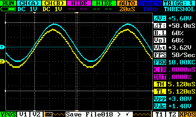
As you can see, the output is a pure sine wave with the frequency 10 KHz (FRQ value in the legend) and the amplitude 3.08V (Vpp value in the legend). The blue line is the output of the DAC8 module, and the yellow line is the output of the DAC12 module. I shifted the yellow plot down to prevent their overlapping, in fact they have the same amplitude and frequency. The only difference is that the DAC12 has a sharper form (we will talk about the reasons later).
So everything already works as desired, and without involvement of the CPU! The rest of the code will be devoted to changing the frequency and the waveform of the signals.
In lines 105-110 we send the commands via RTT about how to control the signal parameters. If you want to change the frequency, you just need to send the number, and it will be considered as the frequency value in Hz. The max frequency that I managed to obtain was 100 kHz but in this case the signal amplitude already became smaller. The min frequency is 
In lines 112-165 there is the main loop of the program, in which we only check if there is any data from the RTT and process it accordingly.
In line 114 we check if there is any data in the RTT buffer by calling the SEGGER_RTT_HasData function.
If there is some data available, we first clear all the elements of the rtt_buf array (lines 116-117). After that we read the data from the RTT buffer into this array using the SEGGER_RTT_Read function (line 118).
Then we check the first character of the received data. If it is a number (line 119) then we suppose that this is the signal frequency. In this case we convert the rtt_buf into the integer value frequency using the standard C function atoi (line 121). Then we update the GPT period using the function R_GPT_PeriodSet (line 122). In line 123 we send the confirmation message via RTT using the SEGGER_RTT_printf function.
If the first character is not a number (line 125) then we check the valid variants using the switch construction (lines 127-162). If the first element of the rtt_buf array is “s” (line 129) then we call the dtc_reconfigure function with the arguments 0 as transfer number and sine_array_8b as the source address (line 130). After that the sine waveform will be set for the first channel. Also we save the address of the sine_array_8b array in the prev_src0 pointer (line 131) (be patient, we will find out why we need this very soon). Then we do the same check with the letters “w” (lines 133-136), “e” (lines 137-140), “d” (lines 141-144) and set the corresponding waveform for the first channel. Then in lines 145-160 we do the same checks for letters “S” (lines 145-148), “W” (lines 149-152), “E” (lines 153-156), and “D” (lines 157-160) which change the waveform of the second channel. If the first character is not a number or one of these four letters, we send a warning about the wrong command (line 161).
This is all about the main function of the program, let’s now return to the dtc_reconfigure function (lines 50-69) which description we skipped.
In line 52 we stop the DTC operation by setting the DTCST bit as 0.
In line 52 we check if the transfer number n is 0. If it is so, then we need to set a new source for DTC transfer 0.
In line 55 there is the following expression:
g_transfer0_cfg.p_info->p_src = (uint8_t *)source;
We are already familiar with the structure g_transfer0_cfg as we met it and considered it in detail in line 88. So in line 55 we set the new source address for transfer 0. As initially the parameter source has the type void, we need to explicitly cast this pointer to the right type, which in the current case is uint8_t*.
In line 56 we set the value of the prev_src1 as the source address of DTC transfer 1.
And now the time has come to explain why there prev_src0 and prev_src1 variables are needed. Even though transfer 0 and transfer 1 are chained, they have their own counters and source and destination addresses. So when we set the new address for transfer 0, transfer 1 will keep counting the transfers from the point where it was interrupted. In this case the signals will become shifted by phase, and this shift is totally unpredictable. To avoid this we assign source addresses of both transfers with the start addresses of the corresponding waveform arrays. And if for transfer 0 we set the new address, for transfer 1 we need to restore the initial one, which was saved in the prev_src1 pointer.
If the value of the n argument is 1 (line 58) we do the opposite thing - set the new source address for transfer 1 (line 60) and restore the initial address for transfer 0 (line 61).
After that in lines 63 and 64 we change another field of the p_info structure - length which is the number of transfers in the repeat transfer mode. We must do this because we can interrupt the execution of the DTC at any moment, and the length value continuously changes according to the number of the remaining transfer. And if we don’t reassign it, the module can consider that the number of transfers has been reduced, and distort the waveform. We must do this assignment for both transfers, as after lines 53-62 both source addresses of them are assigned with the start addresses of the corresponding waveform arrays.
Now as we have changed the required values, we can reconfigure both DTC transfers using the R_DTC_Reconfigure function (lines 65 and 66).
Line 67 is similar to line 52 but in it we set the value of the DTCST bit as 1, enabling the operation of the DTC module.
Finally in line 68 we send the confirmation via RTT that all is done.
This time the dtc_reconfigure function is an even greater improvisation than in the previous part. So I ask you again, if there is a better solution of reconfiguring the transfers please let me know in the comments under this tutorial.
And that’s actually all about the program code. As you see, it is not much harder than the previous program even though it’s much longer.
Testing of the Signal Generator
Now the time has come to build the application, connect the board to the PC and run the debug. Also you need to run the “J-Link RTT Viewer” application. I expect that you followed the previous part of this tutorial and have reconfigured the RTT Viewer according to its demands.
Now let’s see how the changing of the waveforms work. Type the “w” in the input field and press the “Send” button to set the saw waveform of the first channel. You should see the following result (Figure 11).
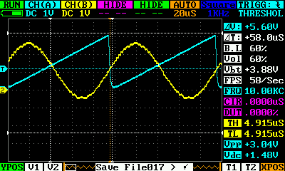
Now let’s send the “E” character to set the triangle waveform in channel 2 (Figure 12).
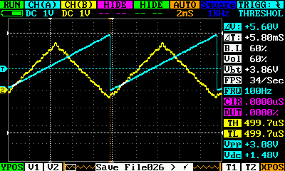
You can send other letters and see the other combinations of waveforms by yourself, everything should work as desired.
Now let’s try to change the frequency of the signal. To do this type a new frequency value, for example, 20000 and see the result (Figure 13).
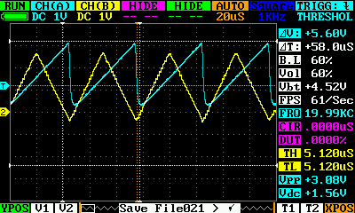
As you can see, the form of the first channel becomes smoother. Initially I thought that it is the oscilloscope probe capacitance that makes the filtering effect and distorts the signal but for DAC12 the signal isn’t distorted even on higher frequencies, and the steps are still noticeable. So this version doesn’t seem to be correct. Now I suspect the board routing is the cause of the increased jaggedness on the DAC12 signal but am unable to figure out why or prove it. The P013 pin merged with the DAC8 output is also used as the VREFH input, and there is even a footprint for a capacitor between VREFH and VREFL pins which is not installed though but probably the routes capacitance itself is enough to distort signal at higher frequencies.
Let’s now try to increase the frequency even more and set it as 100 kHz (Figure 14).
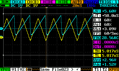
And the attempt fails. The max frequency in this case is just 28.56 kHz (see Figure 14) - almost 4 times slower than the previous time! I didn’t expect such a drastic fall of productivity when using the chained DTC transfer. But we have what we have, and we need to take this fact into account in the future projects - chained transfer is much slower than a standalone one.
And finally let’s set the low frequency, for example, 100 Hz, and see the signal form (Figure 15).
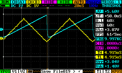
You can see that the saw signal became sharper at the edges even though the steps are still almost not noticeable.
Well, that’s actually all I wanted to say in this tutorial. This time we have acquainted ourselves with one more new module DAC12. We have created a double channel signal generator which can independently produce four different waveforms with frequencies from 1Hz to 28kHz.
In the next tutorial we will start discovering the ADC converters of the RA2A1 MCU.
As homework, I suggest you add the third output channel of the signal generator based on channel 1 of the DAC8 module. Try to add the third DTC transfer and join all three of them into a chain.

Get the latest tools and tutorials, fresh from the toaster.


