Signal Generator using 8-bit DAC, Event Link Controller (ELC), and Data Transfer Controller (DTC) | Renesas RA - 16
Published
Hi there! In the previous tutorial, we familiarized ourselves with two analog comparator modules in the RA2A1 MCUs - high-speed and low-power. Today we will keep discovering the analog peripheral modules, and this time we will consider the digital-to-analog converter (DAC). As I already mentioned, there are two DAC modules in the RA2A1 family - 8-bit and 12-bit options. Both of them are quite similar except for some minor unique features.
In this tutorial we will create the signal generator which will produce sine, saw, triangle or trapezoid waves with the specified frequency. The waveform and the frequency will be set via the SEGGER RTT protocol which we explored in the previous tutorial.
In the first part of the tutorial we will create a single channel generator based on the 8-bit DAC module, and in the second part we will add a second channel based on the 12-bit DAC module.
The most interesting thing is that updating the DAC value and starting the new conversion will be implemented totally without CPU involvement. We will consider the details later in this tutorial. For now let’s, as usual, consider the new MCU modules that will be used in the current project.
Introduction into 8-bit Digital to Analog Converter (DAC8)
Actually, there is not much to talk about. The DAC8 module is a very simple module which generates the output voltage according to the input 8-bit code. If the input signal is 0 then the output voltage is also 0. If the input signal is 255 then the output voltage is AVCC0. And generally the output voltage is calculated as:
Where DACSn is the value written into the register DACSn (n = 0, 1). Speaking of, the DAC8 module has two channels which can be configured separately and independently. That’s why there are two DAC input registers - DACS0 and DACS1.
Normally, if AVCC0 is greater than 2.7V the conversion time is 3us which gives the max theoretical update frequency as 333kHz. If AVCC0 is lower than 2.7V, you need to enable the charge pump generator at the output, and the conversion time in this case doubles - up to 6 us.
The DA conversion can be synchronized with the ADC conversion if you use it. This is done to reduce the noise during the conversion.
The output of the DAC8 can be applied to the output MCU pins, to the built-in operational amplifiers, or be used as the reference voltage for both high-speed and low-power comparators.
The DA conversion can be started by a signal from the ELC module which reduces the power consumption and excludes the CPU from this process. In our current project we will use this feature.
And that’s about it for the DAC8 module. If you want to know more about it, you can refer to the RA2A1 user’s manual.
Introduction into Data Transfer Controller (DTC)
We have already used the DTC module in a previous project: for transferring data to/from touch module in tutorial 6 or I2C module in tutorial 8. But there it was configured automatically without our involvement, and all we had to do was enable its use. This time we will consider it in more detail and configure everything manually.
As I mentioned before, the DTC module is used to transfer the data from one memory region or peripheral module to another one without involvement of the CPU. Its functionality is very similar to the direct memory access (DMA) controller, and in some RA groups both DMA and DTC controllers are present in the same CPU. In the RA2A1 group only DTC is present though.
DTC can operate in three transfer modes:
- Normal transfer mode, in which single activation leads to a single data transfer. If the destination or/and source addresses are declared as incremented/decremented, they change accordingly.
- Repeat transfer mode is similar to the normal transfer mode, but in it the transfer address returns to the start address after the number of data transfers reaches the specified repeat size. This number can be up to 256 transfers.
- Block transfer mode, in which single activation leads to a single block transfer. The max size of the block is 256 x 4 bytes = 1024 bytes.
The DTC transfer can be activated by any of the interrupts generated by the peripheral modules of the MCU. Also, transfers can be chained, which means that the same interrupt source will activate several different transfers which are configured as “chained” (we will talk about this feature in the second part of this tutorial).
The DTC memory area reaches from addresses 0x00000000 to 0xFFFFFFFF which includes 4GB of the memory. This is more than enough for the RA MCUs even in case of connecting external memory chips.
DTC’s data transfer units are: 1 byte, 1 half-word (2 bytes), and 1 word (4 bytes). In the block transfer the max block size is 256 of data transfer units.
The DTC module also can generate its own interrupts: on a DTC activation interrupt, after a single data transfer or after a data transfer of a specified volume. At the same moment it also generates the ELC events.
This probably sounds a bit complex now but when we use it, you will see that it’s even more complex than you anticipated. For more information about DTC please refer to the corresponding chapter of the RA2A1 user’s manual.
Algorithm of the Operation of the Signal Generator
This time, there will not be any schematics diagram, as we will not use any external parts except for the oscilloscope which we will connect to the DAC8 output pin.
But the algorithm of operation needs some more explanation. The block diagram of the signal generator is presented in Figure 1.
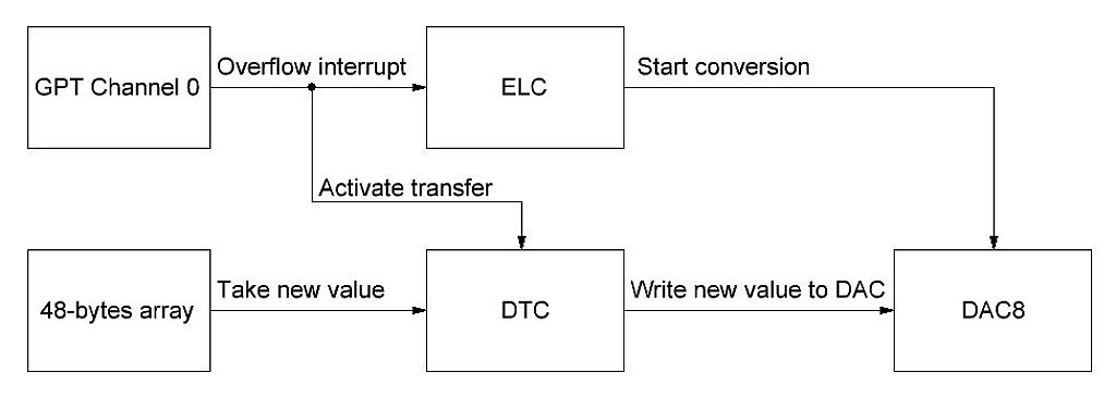
As you see in Figure 1, the “instigator” of everything is GPT. Here I used channel 0 because it is the only one that has the resolution 32 bits which increases the range of the signal frequency. In the program we will set the period of the timer overflow. On overflow, the timer generates the interrupt which is used as an activation source for the DTC module, and simultaneously as the source event for the ELC module.
DTC is configured in the repeat transfer mode with the data transfer unit of 1 byte. In the RAM there are four arrays of 48 bytes each. Each array consists of the values for generating one period of one type of the signal. The number 48 was not selected randomly. By default the GPT timer is clocked with the PCLKD source which in its turn has the default frequency of 48 MHz. And if we generate the waveform with 48 points, it will be easier to calculate the waveform frequency:
Also, 48 points is quite enough to generate the relatively smooth signal which we will see in the oscillograms at the end of this tutorial.
But let’s return to the block diagram in Figure 1. So when the timer overflows, the DTC module takes the next value from one of the four 48-byte arrays and writes it into the DACS0 register of the DAC8 module, which in its turn changes the output voltage. When DTC reaches the last element of the array, it automatically returns to the beginning of the array because it works in the repeat mode, so the new period of the waveform will be output right after the previous one forming a continuous signal.
Simultaneously with sending the new value to DAC8, the ELC module automatically initiates the new DA conversion. Thus we totally eliminate the CPU intrusion into this process: GPT initializes the next step, DTC copies the new data, and ELC starts the DA conversion.
Now, a few words about these 48-byte arrays. As I mentioned before, each of them consists of data to generate one period of the corresponding waveform: sine, saw, triangle, or trapezoid.
For sure, we can calculate the new values on the fly but this will involve the CPU in the generation process and slow it down because the mathematical calculations take some time (especially for a sine wave). So I have calculated everything for you, and you can use these values as you need. If you want to make your own waveform, you need to remember that the minimum DAC8 value is 0, and the maximum value is 255, so you need to shrink or expand your values to this range.
Let me show an example of the generation of the sine waveform. As you know the sin(x) function has the ranges [-1; 1], so -1 of the sin(x) should correspond to 0 of DAC8, and 1 of sin(x) should correspond to 255 of DAC8. Here we can use the formula of linear interpolation:

As we know, the sinusoidal period is 2, and if we calculate the DACS0 values for 
The same with other waveforms. The most complex was the trapezoid form, as it required linear interpolation for each line segment. I won’t reproduce all the calculations here, you can treat it as an exercise in mathematical calculations by yourself if you want. As it is, you can see all the data points within the program code itself.
Project Creation and Configuration
I think now it’s enough information to start with the project. So let’s open e2 studio and create a regular project based on C language using the “Bare Metal - Minimal” template.
First, we will switch to the “Pins” tab and configure the single pin we will use in the current project - the DAC8 output. So we need to scroll down the “Pin selection” list, find and expand the “Analog:DAC8” sublist and select the line “DAC80” which corresponds to the channel 0 of the DAC8 module. Here we only need to change the “Operation mode” from “Disabled” to “Enabled” and see that the “DA” value now has become “P013” (Figure 2).

There is nothing more to be done here, so we can switch to the “Stacks” tab, add and configure the required stacks. As follows from Figure 1, we will need the GPT, ELC, DAC8, and DTC stacks. Let’s add them one by one in this sequence.
We already have considered the GPT timer in detail in tutorial 6 about PWMs, so you already know how to add its stack. Now let’s select the “g_timer0 Timer, General PWM (r_gpt)” block and configure it according to Figure 3.

As you can see, here we change only a few things - we reduce the timer period to 100 ticks, so now the default waveform frequency will be
Also, we need to change the “Overflow/Crest Interrupt Priority” from “Disabled” to “Priority 1” (actually you can use any priority, there’s nothing to conflict with). In this way we enable the timer overflow interrupt which will be used by the DTC module. Please note that we don’t set the callback name as we’re not going to process the interrupt by the CPU.
Then we need to add the ELC stack which is located inside the “System” list (I talked about it in tutorial 14). This stack doesn’t require any configuration, so let’s now add the DTC stack which is located in the “Transfer” list and called “Transfer (r_dtc)” (Figure 4).

Let’s select the block “g_transfer0 Transfer (r_dtc)”. Now none of its parameters are blocked (unlike previous times we used it), and we can configure it as we want (Figure 5).

Let’s briefly consider all the parameters of this module.
- “Linker section to keep DTC vector table” speaks for itself. This is the memory section defined in the “fsp.ld” file, in which the DTC vector table is located. Unless you totally understand what you are doing, I’d strongly recommend not to change the default value “.fsp_dtc_vector_table”. I think I owe you some explanation here. The MCU has a single DTC module but it can be configured several times to perform different transfers. To do the trick, there is a special memory region - DTC vector table, in which all the configurations are stored, and if a legitimate activation source is triggered then the DTC knows which transfer corresponds to it, and performs this transfer.
- “Name” as usual means the name of the current DTC stack in the program. We can leave it as default.
- “Mode” selects the DTC transfer mode. I already talked about them earlier, and explained why we need to select the “Repeat” mode.
- “Transfer size” is the data transfer unit. Here we need to change this value to “1 Byte” as we send only one byte at a time.
- “Destination Address Mode” selects whether the destination address will be fixed, or incremented or decremented after each transfer. In our case we will send the data to the DACS0 register whose address is fixed, so we leave this parameter unchanged.
- “Source Address Mode” selects whether the source address will be fixed, or incremented or decremented after each transfer. As we are using the array of data as the source, we need to increment the address after each transfer, so we changed this value to “Increment”.
- “Repeat Area (Unused in Normal Mode)” selects whether the source or destination address should be returned to the initial value after completion of the specified number of transfers. In our case we need to return to the beginning of the array, so we select “Source” here.
- “Destination Pointer” is the memory address into which the data will be transferred. We can leave it as “NULL” for now and configure it in the code.
- “Source Pointer” is the memory address from which the data will be transferred. We can leave it as “NULL” for now and configure it in the code.
- “Interrupt Frequency” allows the DTC interrupts to generate either “After all transfers are completed” or “After each transfer”. In the current case, there is no difference for us but let’s leave the “After all transfers are completed” option to reduce the interrupt frequency.
- “Number of Transfers” sets the number of transfers in the repeat transfer mode. As we agreed, we need to set it as 48.
- “Number of Blocks (Valid only in Block Mode)” sets the number of blocks to transfer in the block mode.
- “Activation Source” selects the interrupt that will activate the transfer. For now, we have enabled only one interrupt - “GPT0 COUNTER OVERFLOW”, so at this moment, this is the only available option. And luckily for us, it’s the exact option that we need.
That’s everything for the configuration of the DTC stack. If you want to read more information about it, please refer to the official FSP documentation.
And now we can add the last stack - DAC8. To do this, we need to expand the “Analog” list and select the “DAC8 (r_dac8)” line (Figure 6).

After that, the “g_dac0 DAC8 (r_dac8)” block will appear, which we need to configure according to Figure 7.

As you can see, the DAC8 stack has quite few parameters:
- “Name” is still the name of this stack in the program, we’ll leave it by default.
- “Channel” selects the DAC8 physical channel. Valid values are 0 or 1. As we will use channel 0, we leave this parameter unchanged.
- “D/A A/D Synchronous Conversion” allows synchronization of the AD and DA conversions to reduce the noise. In our case we don’t use the ADC module, so we can leave this parameter as “Disabled”.
- “DAC Mode” selects between the “Normal mode” in which the conversion starts by the program, and “Real-time (Even Link) Mode” in which the conversion starts by the ELC module when the corresponding event happens.
- “Real-time Trigger Event” selects the event which starts the DA conversion if in the previous line you selected “Real-time (Even Link) Mode”. We have agreed (see Figure 1) that we will use the GPT overflow event as a trigger, so we need to find and select the “GPT0 COUNTER OVERFLOW (Overflow)” event.
- “Charge Pump (Requires MOCO active)” enables or disables the charge pump at the DAC8 output. In our case the AVCC0 voltage is greater than 2.7V, so we can disable it to decrease the conversion time.
Make sure that the “DA” pin is set as “P013”.
Here is all about the configuration of the DAC8 module. As usual, for more information about it please refer to the Renesas FSP documentation.
After all configurations your Stacks Configuration should look like in Figure 8.

Now let’s switch to the “Event Links” tab and make sure that in the “Allocation” table the DAC80 function is linked with the “GPT0 COUNTER OVERFLOW (Overflow)” event (Figure 9).

We have configured everything we could here, so now we can click the “Generate Project Content” button and switch to the program code writing.
Program Code of The Project
Before we proceed with creating our own code, we need to add the files for supporting the RTT. I have explained in detail how to do this in the previous tutorial, so please refer to it. Also, if you follow all the tutorials, you can just copy and paste the RTT-related files from the previous project into the current one.
And now we can open the “hal_entry.c” file and write the program code.
#include "hal_data.h"
#include "SEGGER_RTT.h"
#include <stdlib.h>

FSP_CPP_HEADER
void R_BSP_WarmStart(bsp_warm_start_event_t event);
FSP_CPP_FOOTER

uint8_t sine_array_8b[48] = {128, 144, 160, 176, 191, 205, 218, 229, 238, 245, 251, 254, 255, 254, 251, 245,
238, 229, 218, 205, 191, 176, 160, 144, 128, 111,  95,  79,  64,  50,  37,  26,
17,  10,   4,   1,   0,   1,   4,  10,  17,  26,  37,  50,  64,  79,  95, 111};

uint8_t saw_array_8b[48] = {  0,   5,  11,  16,  22,  27,  33,  38,  43,  49,  54,  60,  65,  71,  76,  81,
87,  92,  98, 103, 109, 114, 119, 125, 130, 136, 141, 146, 152, 157, 163, 168,
174, 179, 184, 190, 195, 201, 206, 212, 217, 222, 228, 233, 239, 244, 250, 255};

uint8_t triangle_array_8b[48] = {  0,  11,  21,  32,  43,  53,  64,  74,  85,  96, 106, 117, 128, 138, 149, 159,
170, 181, 191, 202, 213, 223, 234, 244, 255, 244, 234, 223, 213, 202, 191, 181,
170, 159, 149, 138, 128, 117, 106,  96,  85,  74,  64,  53,  43,  32,  21,  11};

uint8_t trapezoid_array_8b[48] = {128, 144, 160, 176, 192, 207, 223, 239, 255, 255, 255, 255, 255, 255, 255, 255,
255, 239, 223, 207, 192, 176, 160, 144, 128, 112,  96,  80,  64,  48,  32,  16,
0,   0,   0,   0,   0,   0,   0,   0,   0,  16,  32,  48,  64,  80,  96, 112};

void dtc_reconfigure (uint8_t* source); //Declaration of the dtc_reconfigure function

void dtc_reconfigure (uint8_t* source)  //Reconfigure the source of the DTC module
{
    R_DTC->DTCST_b.DTCST = 0;       	//Disable the DTC transfers
    g_transfer0_cfg.p_info->p_src = source; //Set the new source
    g_transfer0_cfg.p_info->length = 48;	//Set the number of transfers as 48
    R_DTC_Reconfigure(&g_transfer0_ctrl, g_transfer0_cfg.p_info); //Reconfigure the DTC module
    R_DTC->DTCST_b.DTCST = 1;       //Enabled the DTC transfers
    SEGGER_RTT_printf(0, "Done\r\n");   //Send confirmation via RTT
}

/*******************************************************************************************************************//**
 * main() is generated by the RA Configuration editor and is used to generate threads if an RTOS is used.  This function
 * is called by main() when no RTOS is used.

 **********************************************************************************************************************/
void hal_entry(void)
{
    char rtt_buf[10];               	//Buffer to receive the data via RTT
    R_ELC_Open(&g_elc_ctrl, &g_elc_cfg);	//Open the ELC stack
    R_ELC_Enable(&g_elc_ctrl);          	//Enable ELC

    R_DAC8_Open(&g_dac8_0_ctrl, &g_dac8_0_cfg); //Open the DAC8 stack
    R_DAC8_Start(&g_dac8_0_ctrl);       	//Start DAC8 conversions

    R_DTC_Open(&g_transfer0_ctrl, &g_transfer0_cfg);//Open the DTC stack
    R_DTC_Reset(&g_transfer0_ctrl, sine_array_8b, (void*)&R_DAC8->DACS[0], 48); //Set the source and destination addresses
    R_DTC_Enable(&g_transfer0_ctrl);	//Enable DTC

    R_GPT_Open(&g_timer0_ctrl, &g_timer0_cfg); //Open the GPT stack
    R_GPT_Start(&g_timer0_ctrl);    	//Start GPT counting
    //Information about the controls sent via RTT
    SEGGER_RTT_printf(0, "Type a number to set the frequency in Hz (Max is 100 kHz)\r\n");
    SEGGER_RTT_printf(0, "Type \'s\' to output the sine wave\r\n");
    SEGGER_RTT_printf(0, "Type \'w\' to output the saw wave\r\n");
    SEGGER_RTT_printf(0, "Type \'e\' to output the triangle wave\r\n");
    SEGGER_RTT_printf(0, "Type \'d\' to output the trapezoid wave\r\n");

    while (1)
    {
        if (SEGGER_RTT_HasData(0)) //If we received some data via RTT
        {
            for (uint8_t i = 0; i < sizeof (rtt_buf); i ++)
                rtt_buf[i] = 0; 	//Set all elements of the rtt_buf array as 0
            SEGGER_RTT_Read(0, rtt_buf, sizeof (rtt_buf)); //Read the received data into rtt_buf
            if ((rtt_buf[0] >= '0') && (rtt_buf[0] <= '9')) //If the first character is digit
            {
                int frequency = atoi(rtt_buf);  //Then convert the buffer content into the number
                R_GPT_PeriodSet(&g_timer0_ctrl, (uint32_t)(1000000 / frequency)); //And sen new GPT frequency
                SEGGER_RTT_printf(0, "Done\r\n"); //Send confirmation via RTT
            }
            else //If the first character is not a digit
            {
                switch (rtt_buf[0])
                {
                    case 's': dtc_reconfigure(sine_array_8b); break; //If 's' was received, set sine wave
                    case 'w': dtc_reconfigure(saw_array_8b); break; //If 'w' was received, set saw wave
                    case 'e': dtc_reconfigure(triangle_array_8b); break; //If 'e' was received, set triangle wave
                    case 'd': dtc_reconfigure(trapezoid_array_8b); break; //If 'd' was received, set trapezoid wave
                    default: SEGGER_RTT_printf(0, "Wrong command\r\n"); break; //Otherwise inform about the wrong command
                }
            }
        }
    }

#if BSP_TZ_SECURE_BUILD
    /* Enter non-secure code */
    R_BSP_NonSecureEnter();
#endif
}
The code is a bit longer than in the previous tutorial but it’s because of the arrays’ declarations, the essential part is still quite short and clear.
In line 2 we include the “SEGGER_RTT.h” file to be able to use the RTT functions. In line 3 we include the standard C header “stdlib.h” in which the atoi function used in line 73 to convert the string into the integer number is declared.
In lines 9-23 there is declaration of the waveform arrays: sine_array_8b (lines 9-11), saw_array_8b (lines 13-15), triangle_array_8b (lines 17-19), trapezoid_array_8b (lines 21-23).
In line 25 we declare the function dtc_reconfigure which changes the source address of the DTC module. This function has only one argument - source which represents the pointer to one of the declared earlier arrays. The body of the dtc_reconfigure function is located in lines 27-35 but let’s skip it for now and return to it after consideration of the main function hal_entry (lines 41-95).
In line 43 we declare the local array rtt_buf of 10 elements of char type. It will be used to receive the data from the RTT.
In lines 45-46 we open and enable the ELC stack, after which all the links from the “Allocation” table (Figure 9) become active. In our case, the DAC8 start conversion function becomes linked to the GPT0 overflow event.
In line 48 we open the DAC8 stack, and in line 49 we start the DA conversion by invoking the function R_DAC8_Start. If the DAC module would be converted in the normal mode (Figure 7) the conversion would start at once but as we selected the event link mode, it will start from the ELC signal.
In line 51 we open the DTC stack. In line 52 we set the source and the destination addresses along with the number of transfers using the R_DTC_Reset function. It has four arguments:
- pointer to the transfer_ctrl_t structure which is used to control DTC in the program, in our case it’s the g_transfer0_ctrl which has been created by the FSP configurator;
- pointer to the source address from which DTC will take the data, in our case it’s the sine_array_8b which points at the first element of the eponymous array.
- pointer to the destination address to which DTC will transfer the data, in our case it’s the DACS0 register of the DAC8 module. In the program all modules are accessible via the prefix “R_” followed by their names: R_DAC8. This is the structure in which one can directly access the registers of the module. As I said before we need the register called DACS0, and in the R_DAC8 structure it’s called as DACS[0];
- number of transfers in the repeat transfer mode, in our case it’s 48.
In line 52 we enable the DTC transfers by invoking the function R_DTC_Enable.
In line 55 we open the GPT stack, and in line 56 we start the timer counting.
After line 56 the program becomes fully functioning. You can check this by commenting out the rest of the lines. If you now connect the oscilloscope to the pin P013 which is merged with the “VREFH” function in the J3 header, you will see the following (Figure 10).

As you can see, the output is a pure sine wave with the frequency 10 KHz (FRQ value in the legend) and the amplitude 3.12V (Vpp value in the legend).
So everything already works as desired, and without involvement of the CPU! The rest of the code will be devoted to changing the frequency and the waveform of the signal.
In lines 58-62 we send the commands via RTT about how to control the signal parameters. If you want to change the frequency, you just need to send the number, and it will be considered as the frequency value in Hz. The max frequency that I managed to obtain was 100 kHz but in this case the signal amplitude already became smaller. The min frequency is 
In lines 64-89 there is the main loop of the program, in which we only check if there is any data from the RTT and process it accordingly.
In line 66 we check if there is any data in the RTT buffer by calling the SEGGER_RTT_HasData function. It has only one argument - the number of the RTT channel, and returns the number of the bytes in the buffer.
If there is some data available, we first clear all the elements of the rtt_buf array (lines 68-69). After that we read the data from the RTT buffer into this array using the SEGGER_RTT_Read function (line 70). It has three arguments: the number of the RTT channel (0 in our case), the pointer to the buffer to read the data (rtt_buf in our case), and the size of the buffer which we calculate using the standard C function sizeof.
Then we check the first character of the received data. If it is a number (line 71) then we suppose that this is the signal frequency. In this case we convert the rtt_buf into the integer value frequency using the standard C function atoi (line 73). Then we update the GPT period using the function R_GPT_PeriodSet (line 74). It has two arguments: the pointer to the GPT control structure (g_timer0_ctrl in our case), and the period in raw counts, which follows from the formula I provided above:

In line 75 we send the confirmation message via RTT using the SEGGER_RTT_printf function which we are already familiar with.
If the first character is not a number (line 77) then we check the valid variants using the switch construction (lines 79-86). If the first element of the rtt_buf array is “s” then we call the dtc_reconfigure function with the argument sine_array_8b (line 81). After that the sine waveform will be set. Then we do the same check with the letters “w” (line 82), “e” (line 83), and “d” (line 84) and set the corresponding waveform. If the first character is different from these four letters or a number, we send the warning about the wrong command (line 85).
This is all about the main function of the program, let’s now return to the dtc_reconfigure function (lines 27-35) which description we skipped.
In line 29 there is an expression R_DTC->DTCST_b.DTCST = 0. As I already mentioned, the prefix “R_” followed by the module name allows addressing to its registers directly. In the current case we want to change the register of the DTC module. According to the RA2A1 user’s manual, DTCST is the module start register which has only one eponymous active bit. If this bit is 0, the DTC module is stopped, and if it’s 1 then it’s started. For some reason I didn’t find any FSP function which makes such a simple thing, so I had to find out how to stop the module by directly manipulating its registers. So, now we see that after line 29 the DTC module is stopped, and all transfers are stopped as well. If we don’t do this, then during its reconfiguration the transfers continue, and the start address won’t match the address of the first element of the array. In this case the form will be distorted, so during the reconfiguration you better stop the DTC operation.
In line 30 there is the following expression:
g_transfer0_cfg.p_info->p_src = source;
If you are attentive enough, you could notice the g_transfer0_cfg structure in the R_DTC_Open function (line 51). This structure is automatically created by the FSP configurator and already is preset with the values that we write during the configuration of the corresponding stack (Figure 5). The g_transfer0_cfg has a nested structure p_info of the transfer_info_t type. This p_info structure has all the required information about the current transfer (you can find its declaration in the “/ra/fsp/inc/api/r_transfer_api.h” file), and we can change it at any moment if needed (which we actually are doing now). So in line 30 we change the value of the field p_src, which is the pointer to the source address of the DTC module. We assign it with the value source which is the address of the first element of the corresponding waveform array.
In line 31 we change another field of the p_info structure - length which is the number of transfers in the repeat transfer mode. We must do this because we can interrupt the execution of the DTC at any moment, and the length value continuously changes according to the number of the remaining transfer. And if we don’t reassign it, the module can consider that the number of transfers has been reduced, and also distort the waveform.
Now as we have changed the required values, we can reconfigure the DTC module using the R_DTC_Reconfigure function (line 32). It has two arguments - the pointer to the DTC control structure (g_transfer0_ctrl in our case), and the pointer to the transfer_info_t structure (g_transfer0_cfg.p_info in our case).
Line 33 is similar to line 29 but in it we set the value of the DTCST bit as 1, enabling the operation of the DTC module.
Finally in line 34 we send the confirmation via RTT that all is done.
Actually the whole dtc_reconfigure function was just my improvisation and is the result of the trial and error method - I couldn’t find any information about how to reconfigure the DTC module correctly. This function works fine, but if you have a better solution, please share it in the comments.
And that’s actually all about the program code. As I said before, it’s not that complex (except for the dtc_reconfigure function, probably).
Testing of the Signal Generator
Now the time has come to build the application, connect the board to the PC and run the debug. Also, you need to run the “J-Link RTT Viewer” application (I explained how to run and configure it in the previous tutorial). But now we need to perform some additional configurations. First, we need to select the “Input” from the main menu, then expand the “Sending…” list and change the “Send on input” to “Send on Enter” (Figure 11).
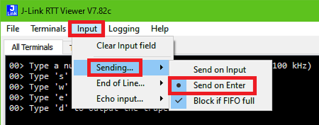
Previously we sent a single character, and it was sent automatically immediately after typing (“Send on Input” option). But now we need to send the number which consists of several characters in one packet, so we first enter the whole number then press the “Send” button to send it to MCU.
Second, we need to select the same “Input” from the main menu, but this time expand the “End of Line…” list, and change it to the “None” (Figure 12).
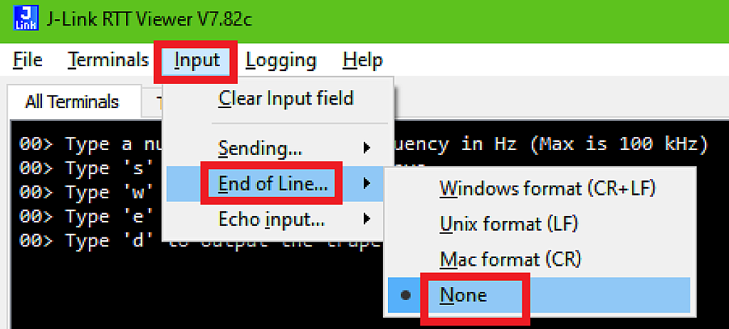
As you can see, the RTT Viewer can automatically add the CR or LF or both to the end of the line. We don’t need it now because it can affect the operation of the atoi function and also overflow the rtt_buf array if the entered frequency is too long. In other applications, this automatic ending of line may be very useful.
Now let’s see how changing the waveforms works. Type the “w” in the input field and press the “Send” button (Figure 13).

You will see the saw waveform now (Figure 14).

Now, let’s send the “e” character and see the triangle waveform (Figure 15).

Finally, let’s type “d” to see the trapezoid signal (Figure 16).

As you can see, changing the waveform works pretty well.
Now let’s try to change the frequency of the signal. To do this type a new frequency value, for example, 20000 and see the result (Figure 17).

As you can see, the signal becomes smoother. I think this is related to the probe capacitance which on such frequencies works as a filter. The filtering effect becomes even more noticeable if we set the higher frequency. In fig 18 you can see the trapezoid signal with the 100 kHz frequency.

As you can see, now it looks like a pure sine signal, also the amplitude of the signal has reduced. To check the theory of the filtering effect, let’s set the low frequency, for example, 100 Hz, and see the signal form (Figure 19).

As you see, now the steps are very noticeable, and the signal form became sharper. This proves the theory of the filtering of the signal at higher frequencies. My assumption is that the input of the oscilloscope has a very high impedance, and even the small capacitance of the probe is enough to save the charge, and operate as a filter enough to distort the signal.
Well, that’s actually all I wanted to say in this tutorial. This time we have acquainted ourselves with the two new modules - DAC8 and DTC. We have created a signal generator which can produce four different waveforms with frequencies from 1Hz to 100kHz. In the second part of this tutorial we will discover the 12-bit DAC module and consider how to make the DTC module operate in the chain mode.
As homework, I suggest two tasks:
- Create your own waveform and add it to the current signal generator.
- Make changes in the program from tutorial 14, removing the external divider R1-R2 and generating the reference voltage of the comparator with the DAC8 module.

Get the latest tools and tutorials, fresh from the toaster.


