e2 studio and FSP Visual Configurator | Renesas RA - 4
Published
Hi again! It’s been a 3 months break since the last RA tutorial I’ve written. A lot of events have happened during this time. Russia started the war in my country, and supply chains have been disrupted, so I couldn’t get any RA board to work with. Finally, a couple days ago, I received the EK-RA2A1 evaluation kit and now can continue with the tutorials. In the meantime, I didn’t sit around without working, and have made several tutorials about the PIC MCUs, which you can find on circuitbread.com as well.
Anyway, let’s continue with the RA family and the FSP. In the previous tutorial we’ve considered the theory of the FSP and considered the “Blinky” project that e2 studio creates automatically. This time let’s consider the e2 studio interface in more detail.
By the way, since the last time Renesas has released the new e2 studio and FSP versions. So now the latest version here https://github.com/renesas/fsp/releases is “fsp_v3_7_0_e2s_v2022-04”. Please update it as I’ll further work with it. The installation process has been described in this tutorial.
After installing and running the updated e2 studio IDE you should select the same Workspace as the previous time. In this case, the formerly created project “Test” will appear in the Project explorer. Upon running it for the first time, it will give a warning that FSP 3.5.0 is not available anymore and suggest to switch to the FSP 3.7.0. You should agree with this proposition. After that your IDE will look like this (Figure 1).
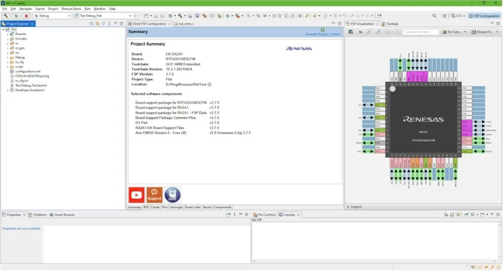
Please note, that in the Project summary, FSP version everywhere is 3.7.0.
The e2 studio, as I mentioned before, is based on Eclipse IDE. And it inherited all its benefits and flaws. As the main benefit I’d mention the extreme flexibility: you can adjust the appearance of the IDE in the way you need. Also it has some features that simplifies the programmer’s life, like autocomplete of the text, pop-up function code view, etc.
As for me, the big flaw of Eclipse is its ponderousness: even on my quite new laptop it works slowly.
The appearance of the e2 studio IDE can be simply adjusted with the use of the perspectives. By default the IDE opens with the “FSP Configuration” perspective (Figure 2).
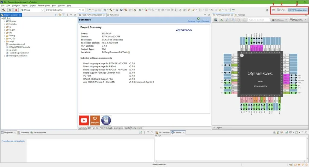
I highlighted the perspectives selector with the red frame. As you see, by default, the “FSP configuration” (3 in Figure 2) is selected. In this perspective you can see the “FSP configuration” window in the center about which we will talk in detail later. To the right of it there is the “FSP Visualization” window in which you can see the MCU package and the configuration of each pin. To get more information about the colors of the pins you can open the “Legend” which is located right after the MCU package. We will spend a lot of time in this perspective.
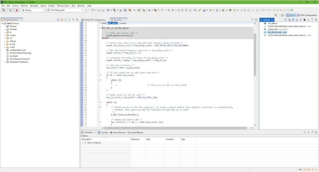
The next perspective that can be used is “C/C++” (2 in Figure 2). If you select it, the appearance of the IDE will change. In this perspective it’s convenient to edit the code, as it provides the code outline which allows you to navigate your code in a fast way. So please switch to this perspective and open the “hal_entry.c” file, where you will see the following (Figure 3).
If you need more perspectives, you can click on button Open Perspective (1 in Figure 2), you will ses the following list (Figure 4).

As you see, the list is quite large but at the first time you will need only “Debug” in addition to the first two. So you can select it to add the button “Debug” to the toolbar.
Now, let’s switch to the “FSP configuration” perspective and consider the FSP configuration window in detail. You can see that at the bottom of this window there are several tabs (red frame in Figure 5).
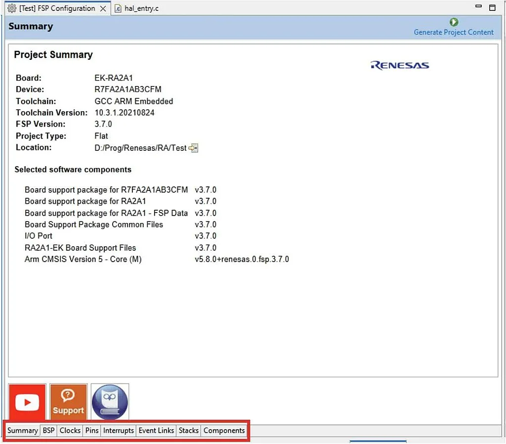
So, in the “Summary” tab which you see in Figure 5, there is (without any surprise) the project summary. There are software and components versions, selected board, MCU, and toolchain. In the bottom part there are useful links to YouTube, Knowledge Base and the FSP documentation that help you to get more information about the RA MCUs and FSP.
The next tab, “BSP” (Figure 6) you can select the FSP version (if several of them are installed), the board, and the MCU.
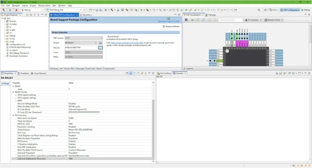
Also you can see the “Properties” window in the left bottom, where you can change some project properties, like stack or heap size, oscillator source, some security options etc. For now let’s leave everything unchanged.
In the “Clock” tab you can see the graphical representation of the clock system of the MCU (Figure 7).
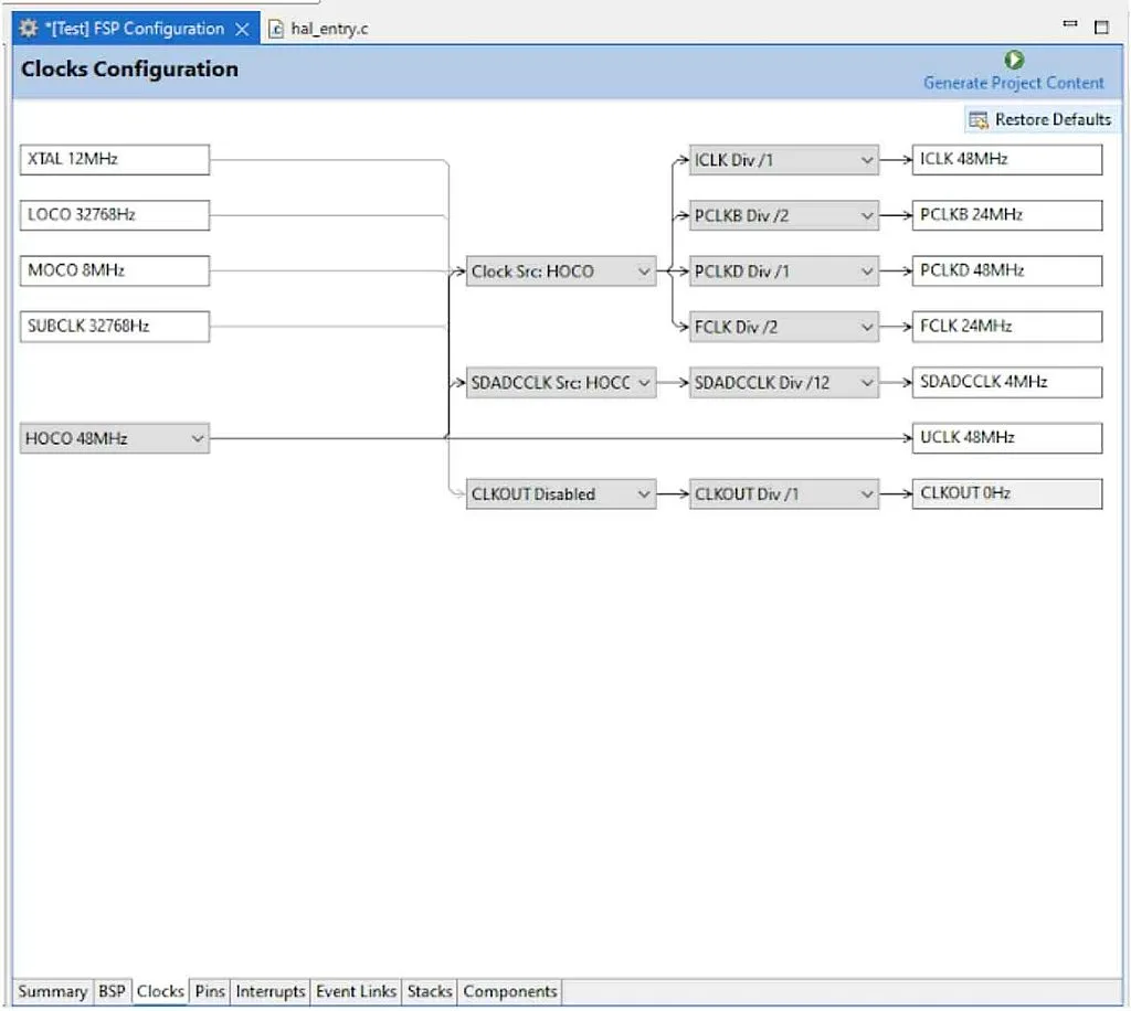
Here you can change the clocking configuration by selecting the sources and the dividers with the drop-down lists. If something goes wrong, and you select the inappropriate values, it will be highlighted with the red color, and the explanation of the problem will appear. For now we will not dwell on the clocking system in detail but consider it in one of the following tutorials.
The next tab “Pins” (Figure 8) allows the initial configuration of the IO pins of the MCU.
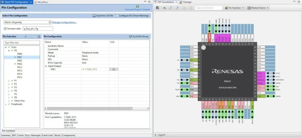
The pins can be sorted either by ports or by peripherals. The changes in this tab immediately are reflected in the FSP visualization window. As you see in Figure 8, as soon as we select the P001 pin, it becomes highlighted in the package view. If there are some pin conflicts, they are shown in the Problems View and in Pin Conflicts View.
The next tab, “Interrupts” allows us to configure the interrupts generated by the MCU core and peripherals and created by the FSP module in the “Stack” tab. We will not consider this tab here, as now it’s empty, and there’s nothing to see there at the moment.
The “Event Links” tab is similar to the previous one. Here we can configure a special Event Link Controller (ELC) which allows the peripheral modules to communicate between each other without the CPU involvement. This means that if some interrupt is generated it can affect the other module directly via ELC, and not use the CPU for this. We will consider this feature in another tutorial as it’s quite useful.
The “Stack” tab (Figure 9) allow to add and configure threads and stacks within the RA project.
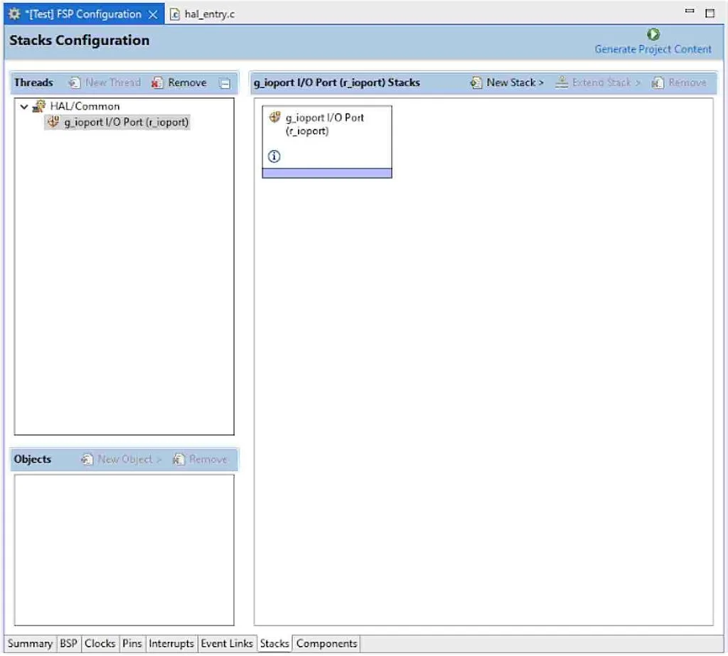
As you see, now we have only one stack - “r_ioport” because in our project we use only the IO port to blink the LED. You can click on the “New Stack” button and see that there are plenty of stacks and threads sorted by categories and peripherals. Some of them are used for configuring the MCU peripheral and have the prefix “r_”, the others are quite advanced and allow us to operate with the motors or specific sensors, their prefix is “rm_”.
The stacks use this naming convention because you can create the stack of the modules dependent on each other. We will consider this in the next tutorial, for now, just believe me.
The last tab “Components” allows us to see and select the FSP components (Figure 10).
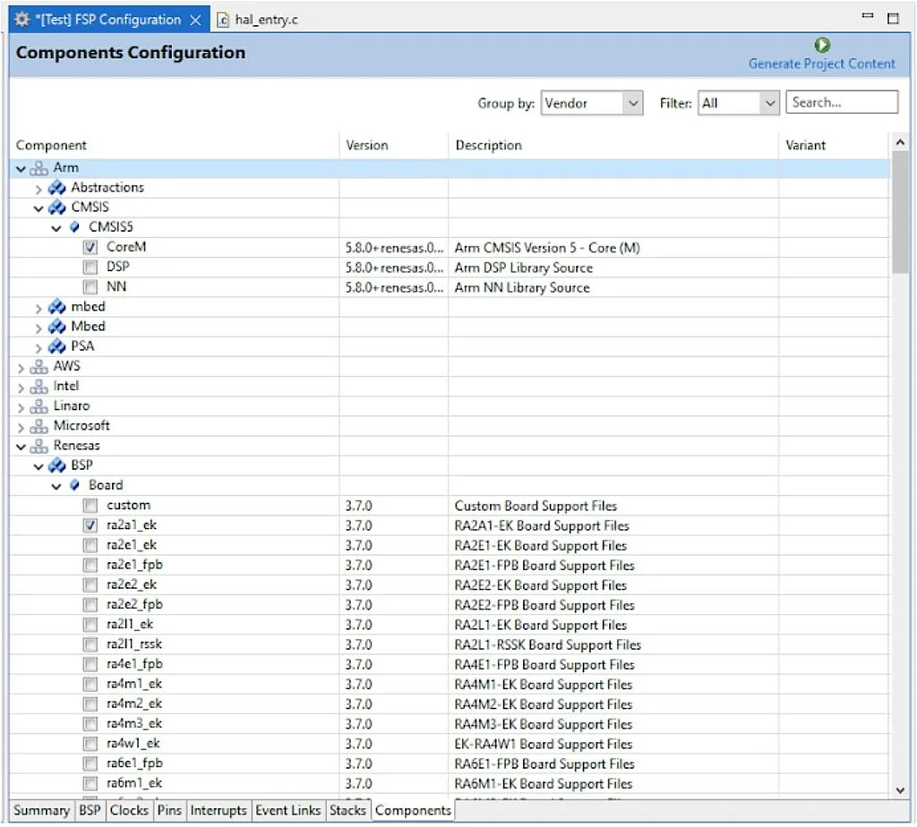
Actually, this tab’s necessity is doubtful for me because it’s recommended to add the new components in the “Stack” tab. But probably there are some very specific components which can be added only here.
And that’s all that I wanted to tell you now about the FSP configurator. I realize that so far a lot of things are not clear for you but the goal of this tutorial is to familiarize you with the e2 studio, so you can easily find the required things there. Clarification will come with time.
Now, let’s finally do some practical work, and connect the development board to the PC. As I said before, my board is EK-RA2A1, so I’ll talk about it. This board has two micro-USB ports: “DEBUG USB” and “DEVICE USB”. As we want now to debug our code, we need to connect the cable to the first port.
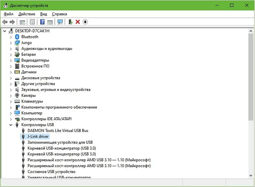
The required driver should be installed automatically. You can make sure of this by opening the Device Explorer and seeing the “J-Link driver” under the “Universal Serial Bus Controller” drop-down list (Figure 11).
Now, we can debug our project but prior to this we need to create the debug configuration. To do this you need to click the arrow near the bug icon and select “Debug Configurations…” in the drop-down list (Figure 12).

You will see the following window (Figure 13).
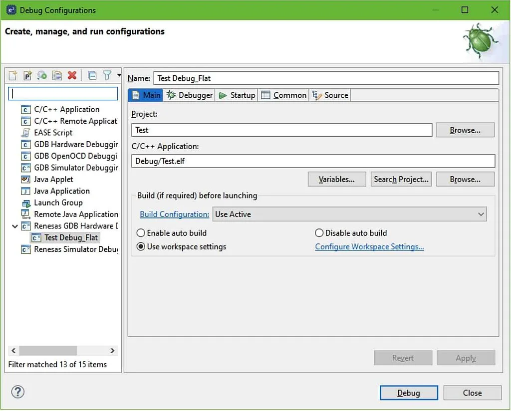
For now we don’t need to change anything there, just make sure that the project name you want to debug matches with your project name. In my case it’s “Test” here and there, so everything is fine. Now, we can click on the “Debug” button. The IDE may ask you if you want to save the changes if there are some unsaved files (Figure 14).

to change the “configuration.xml” file. I will agree because I’m pretty sure I returned everything back to the initial state.
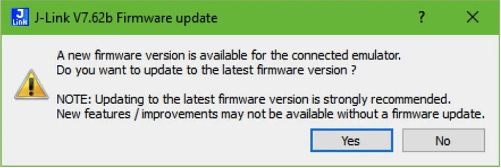
After pressing OK you may be prompted to update the firmware of the J-Link debugger (Figure 15). It’s always a good idea to allow this action.
In several seconds the process will be finished, and you will see the last prompt to switch to the “Debug” perspective (Figure 16). It’s better to do this, and also to set the check “Remember my decision” not to see this prompt again.
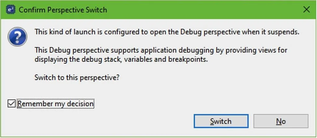
After clicking “Switch”, you will see that the IDE appearance has changed (Figure 17).
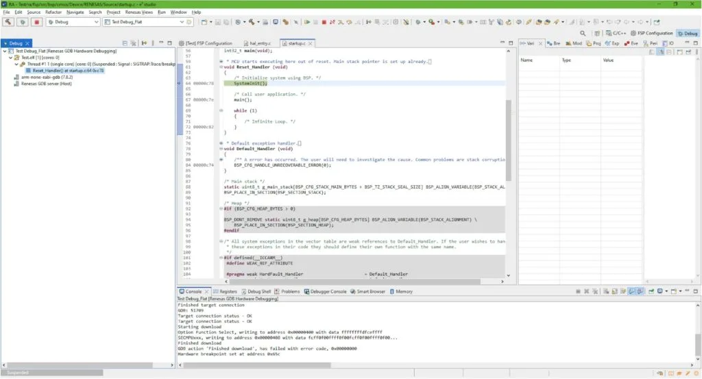
First, in the center you now see the “startup.c” file, as the code execution starts from it. Second, at the right to it, you now see the debugging-related views: Breakpoints, Variables, Expressions, Peripherals, Registers etc. instead of the FSP visualization. Third, an additional toolbar has appeared which allows control of the debugging process.
Initially, the project was stopped at the “SystemInit()” function (see Figure 17). And also you can see that at this moment no LEDs are blinking in your board. To run the project you need to click the “Resume” button which looks like the green triangle or press F8. Now, the project stops at the “hal_entry()” function of the “main.c” file, so you need to press the “Resume” button once again to finally run the project. And tada! The LED is blinking. What a great surprise!
The debugging options here are quite standard: you can pause/resume the program execution, execute the program step-by-step, add/remove the breakpoints, view the variables, registers, memory, expressions when the MCU is paused.
To stop the debugging you need to click the “Terminate” button. I think that's enough for today. We were acquainted with the perspectives of the e2 studio, briefly discovered the FSP visual configurator, and learned how to debug the project.
Next time we will learn how to use the FSP configurator in more detail, and will create the FSP-based project from scratch.

Get the latest tools and tutorials, fresh from the toaster.


