Reverse Biased
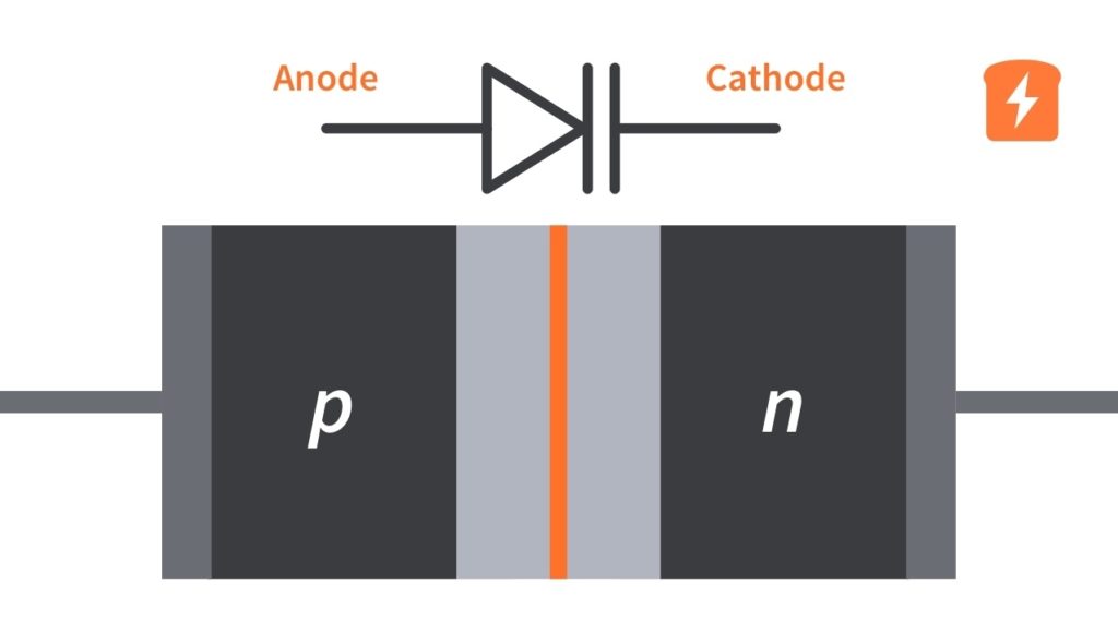
A diode or a pn junction is reverse biased when the negative side of external bias voltage is connected to the p region of the diode (the anode in a diode) and the positive side is connected to the n region (the cathode in a diode). In this condition, the current can’t flow through the pn junction.
VD < 0 - when the diode is operating with reverse bias, we consider the diode “off” or nonconducting because the current is very small.
Microelectronic Circuit Design, 4th Edition by Richard C. Jaeger & Travis N. Blalock
Connecting the p-type region to the negative terminal of the battery and the n-type region to the positive terminal corresponds to reverse bias. If a diode is reverse-biased, the voltage at the cathode is comparatively higher than at the anode. Therefore, very little current flows until the diode breaks down. The connections are illustrated in the adjacent diagram.
Because the p-type material is now connected to the negative terminal of the power supply, the 'holes' in the p-type material are pulled away from the junction, leaving behind charged ions and causing the width of the depletion region to increase. Likewise, because the n-type region is connected to the positive terminal, the electrons are pulled away from the junction, with similar effect. This increases the voltage barrier causing a high resistance to the flow of charge carriers, thus allowing minimal electric current to cross the p–n junction. The increase in resistance of the p–n junction results in the junction behaving as an insulator.
The strength of the depletion zone electric field increases as the reverse-bias voltage increases. Once the electric field intensity increases beyond a critical level, the p–n junction depletion zone breaks down and current begins to flow, usually by either the Zener or the avalanche breakdown processes. Both of these breakdown processes are non-destructive and are reversible, as long as the amount of current flowing does not reach levels that cause the semiconductor material to overheat and cause thermal damage.
This effect is used to advantage in Zener diode regulator circuits. Zener diodes have a low breakdown voltage. A standard value for breakdown voltage is for instance 5.6 V. This means that the voltage at the cathode cannot be more than about 5.6 V higher than the voltage at the anode (though there is a slight rise with current), because the diode breaks down, and therefore conduct, if the voltage gets any higher. This, in effect, limits the voltage over the diode.
Another application of reverse biasing is Varicap diodes, where the width of the depletion zone (controlled with the reverse bias voltage) changes the capacitance of the diode.


