1602 Character LCD - Part 20 Microcontroller Basics (PIC10F200)
Published
Note: Microchip recently made some changes and their newer IDE versions use the XC8 compiler for Assembly, whereas all sample code here is created for the MPASM compiler. However, the sample code has been ported to XC8 by user tinyelect on our Discord channel (to whom we are extremely grateful!) and the XC8 version of the code is at the bottom of this tutorial for your reference. To see the changes needed to switch from MPASM to XC8, please check out the process that he shared.
Hi! This tutorial is going to be somewhat special - it will be the last one in this series. It’s been a long time since the very first tutorial and you’ve discovered a lot in the journey. And in conclusion, I want to show you how to work with the very popular character LCD with 2 lines, 16 characters each (usually just called the “1602 LCD”). This LCD comes with the in-built HD44780 driver (you can read more detail about it here). I will provide you brief information about it, the minimal amount required to initialize the display and show some text on it.
The HD44780 driver uses the 8 or 4 line parallel interface to communicate with the MCU which is not good for us as we have just 3 output pins on the PIC10F200 microcontroller.
To increase the number of the available outputs, we will use the special chip 74HC595 which is an 8-bit shift register (the data sheet can be found here). As you probably know, a shift register is used to convert the sequence of the bits that come to a single serial input into a parallel code which appears simultaneously on whichever outputs you need (in our case, 8). Let’s consider this chip in more detail (figure 1).
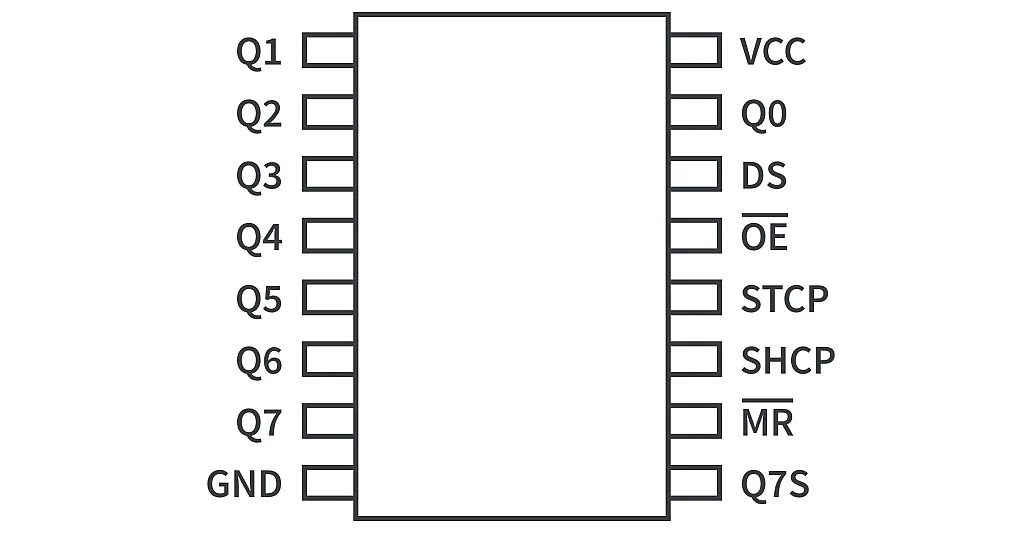
As I mentioned, the chip has a single serial input DS (pin 14) and eight outputs Q0-Q7 (pins 15, 1-7). Also, it has a clock input CHCP (pin 11) on the positive edge of which the data is accepted from the DS input, and the latch input CTCP (pin 12) on the positive edge of which the loaded data appears at the outputs. OE (pin 13) is the output enable pin. If it’s high, then all outputs are in the high-Z mode, and if it’s low, the outputs become active. MR (pin 10) is the reset pin, when it’s low all outputs become 0 regardless of the input. G7S (pin 9) is used to connect several shift registers in series.
As you can see, there are still a lot of inputs and we should decide which of them we will have to connect to the microcontroller. Apparently, the DS and the CHCP pins are mandatory to use. Also, we will use the CTCP pin to prevent an interim result on the output pins. We will connect the OE pin directly to GND, so the outputs will be active all the time, and we will connect the MR pin to the VCC to always keep the shift register in the active mode.
Let’s now see how it works. For instance, we need to transmit the number 0x3A which is 0b00111010 in the binary format. To do this we set the value of the MSB of the number at the DS input, in our case it’s 0. Then we make the pulse on the CHCP input which writes the data. After that, this value will be saved in the Q0 position but will not appear on the real Q0 output until we make the CTCP pulse. Then we shift our number to the right, set the next bit at the DS input (it’s 0 again), and make the CHCP pulse. Now the value from the Q0 will be shifted to the Q1, and the value from the DS will be saved in the Q0 position. We keep doing the same operation eight times to transmit the whole byte. After all the shifts, the MSB will occur at the Q7 position, and the LSB will be at the Q0 position. Now we can make the CTCP pulse in order to latch the outputs and to set the actual values of the bits at the corresponding outputs.
So the algorithm is quite simple: we transmit all eight bits of a byte starting from the MSB bit and then latch the outputs by pulsing the CTCP. Thus, we can have up to eight outputs using a single shift register chip, and also an extra eight outputs adding the next shift registers still using the same three pins of the microcontroller.
You can invent a lot of applications with these shift registers but now we will use this chip just as a tool to control the 1602 LCD. Let’s now consider it in more detail.
There are several displays with the HD44780 driver, they can have different line numbers and position numbers (1x8, 2x8, 1x16, 2x16, 2x20, 4x20 etc.), also they can have different backlight colors (green, yellow, blue, etc.) or don’t have a backlight at all. The character’s color can be black or white. So, as you see, there is a diversity but all of them have the same interface and are controlled using the same commands. I have the display shown in fig. 2 which I bought a long time ago on Aliexpress.
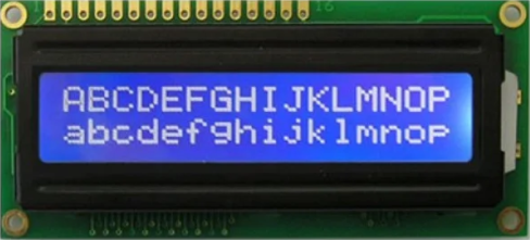
This LCD has the built-in character generator, so you don’t need to design your own characters (like we used to do with the 7-segment indicator). We can just send the ‘A’ letter to the display, and it will be shown - fascinating, isn’t it? Also, the display has 16 empty cells in which you can load your own characters and then use them but we won’t do this in this tutorial. The character generator of the LCDs from Aliexpress usually have a Chinese code page, so you can use the first 128 ASCII characters, which includes capital and small English letters, numbers, and the punctuation signs which is quite good!
Let’s now see which signals has this display (figure 3).
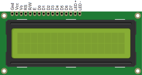
- GND and VCC pins are the power supply of the display. Normally it is 5V.
- The Vo pin is used to set the contrast of the LCD. Usually a potentiometer of 10-47 kOhm is connected to it.
- RS is the data/command input. When this pin is low, the incoming data is considered as a command, and when it’s high, it is considered a character to display.
- RW is the read/write input. When it is low, the data goes from the microcontroller to the LCD, and when it is high, the data goes the reverse direction. As we don’t expect any data from the LCD, we can connect this pin to ground.
- E is the clock input. The data is read on the rising edge at this pin.
- D0-D7 are the data inputs of the 8-bit parallel interface. The HD44780 driver also supports the 4-bit parallel interface. In this case, pins D0-D3 remain unused, and the bytes are transmitted by nibbles: higher one first, lower one second.
- LED+ and LED- are the backlight power inputs. The supply voltage is also 5V, but a series resistor of 22-47 ohms is required.
As for the commands that HD44780 uses, I will not describe them here. You can refer to the data sheet for full information. I will provide you with the information on how to initialize the display which you can use. Also, I’ll show you how to set the cursor position and display some data on the LCD.
Let’s now consider the schematic diagram of the device (figure 4).
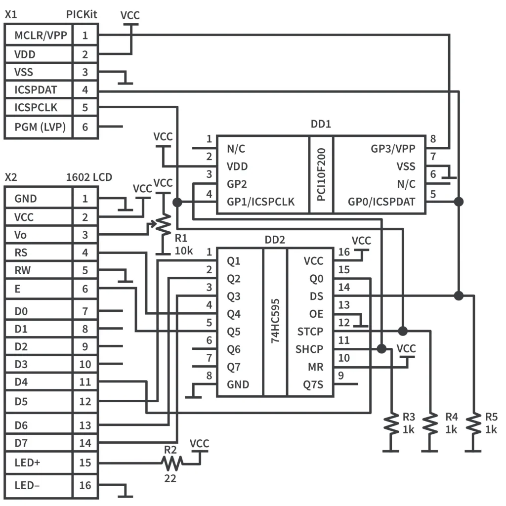
The schematics diagram is quite big but actually the number of the parts is still small. So we have the PIC10F200 microcontroller (DD1) and the programmer (X1). We also have the shift register chip 74HC595 (DD2). The data input DS is connected to the GP0 pin, the clock input CHCP is connected to the GP2 pin, and the latch input CTCP is connected to the GP1 pin. Also, all three pins are pulled down by 1 kOhm resistors R3-R5. This is needed because during the power up, the microcontroller pins act as high-Z inputs. The shift register inputs also have the high impedance. So in this time the random signal levels can happen on these pins, and the behavior of the shift register may become unpredictable. By pulling down the inputs, we hold them low until the microcontroller becomes able to control them.
The 1602 LCD (X2) is connected as described above. The Vo pin is connected to the 10-47 kOhm potentiometer R1. When you power up the device, you should rotate the handle of the potentiometer to make the rectangles of the LCD barely visible. Then the contrast level is set correctly. The LED+ pin is connected to VCC through the 22-47 Ohm resistor R2. The RS, E, D4, D5, D6, and D7 pins are connected to the shift register. Please pay attention that the data pins D4-D7 are connected to the lower four outputs of the shift register Q0-Q3, respectively. The RS input is connected to Q4, and E input is connected to Q5. Thus Q6 and Q7 pins remain unused, and you can expand your device with something else. The RW input of the LCD is connected to the GND, as we will just write to the LCD. The D0-D3 inputs remain unused in the 4-bit interface.
Now let’s consider the program that will initialize the LCD and write the “HELLO WORLD” message, where words will be located in the center of both lines of the LCD.
#include "p10f200.inc"

bit_count    EQU 10    ;counter of the bits
data_byte    EQU 11    ;data byte to send to the shift register
lcd_data     EQU 12    ;byte to send to LCD
data_com     EQU 13    ;if = 0x10, then data, if = 0 then command
temp   	     EQU 14    ;Temporary data
i   		 EQU 15    ;Delay variable
j   		 EQU 16    ;Delay variable
k   		 EQU 17    ;Delay variable

dat   		 EQU    GP0    ;Data input of the shift register
clk   		 EQU    GP2    ;Clock input of the shift register
latch   	 EQU    GP1    ;Latch input of the shift register

RS   		 EQU 4    ;RS signal of the LCD is bit 4
E   		 EQU 5    ;E signal of the LCD is bit 5

    __CONFIG _WDT_OFF & _CP_OFF & _MCLRE_OFF

    ORG 0x0000

INIT
    MOVLW  ~(1<<T0CS)    ;enable GPIO2
	 OPTION

    MOVLW ~((1 << dat) | (1 << clk ) | (1 << latch))
    TRIS GPIO   		 ;Set all pins as outputs
    CLRF GPIO    		 ;Clear GPIO to set all pins to 0
    CLRF data_com   	 ;Set RS line low to send the command

    ;Delay after power-up
    MOVLW 0x07   		 ;Perform delay for 2 second
    CALL DELAY
;-----------LCD initialization------------------
    MOVLW 0x33   		 ;Preparation
    CALL LCD_SEND
    MOVLW 0x02   		 ;Perform delay for 200ms
    CALL DELAY
    MOVLW 0x32   		 ;Set 4-bit interface
    CALL LCD_SEND
    MOVLW 0x28   		 ;Set 2-line display
    CALL LCD_SEND
    MOVLW 0x08   		 ;Display off
    CALL LCD_SEND
    MOVLW 0x01   		 ;Clear display
    CALL LCD_SEND
    MOVLW 0x02   		 ;Perform delay for 200ms
    CALL DELAY
    MOVLW 0x06   		 ;Cursor increment to the right, no shift
    CALL LCD_SEND
    MOVLW 0x0C   		 ;Display on, cursor off
    CALL LCD_SEND
    MOVLW 0x02   		 ;Perform delay for 200ms
    CALL DELAY
;----------End of the initialization part------------------

    MOVLW 0x85   		 ;Set line 1, position 5
    CALL LCD_SEND
    BSF data_com, RS     ;Set RS line high to send the data
    ;Send the word "HELLO"
    MOVLW 'H'
    CALL LCD_SEND
    MOVLW 'E'
    CALL LCD_SEND
    MOVLW 'L'
    CALL LCD_SEND
    MOVLW 'L'
    CALL LCD_SEND
    MOVLW 'O'
    CALL LCD_SEND

    CLRF data_com   	 ;Set RS line low to send the command
    MOVLW 0xC5   		 ;Set line 2, position 5
    CALL LCD_SEND
    BSF data_com, RS     ;Set RS line high to send the data
    ;Send the word "WORLD"
    MOVLW 'W'
    CALL LCD_SEND
    MOVLW 'O'
    CALL LCD_SEND
    MOVLW 'R'
    CALL LCD_SEND
    MOVLW 'L'
    CALL LCD_SEND
    MOVLW 'D'
    CALL LCD_SEND

LOOP   				     ;Main loop of the program

	GOTO LOOP       	 ;loop forever

SEND_BYTE   			 ;Send one byte to the shift register
    CLRF bit_count   	 ;Clear the 'bit_count' register
SEND_BIT   			     ;Send one bit to the shift register
    BCF GPIO, clk   	 ;Set the 'clk' pin low
    NOP   				 ;No operation to implement the instruction
    BCF    GPIO, dat   	 ;Set the 'dat' pin low
    BTFSC data_byte, 7   ;If the MSB of the 'data_byte' is not 0
    BSF GPIO, dat   	 ;Then set the 'dat' pin high
    RLF data_byte, F     ;Shift 'data_byte' to the left
    BSF GPIO, clk   	 ;Set the 'clk' pin high
    INCF bit_count, F    ;Increment the 'bit_count'
    BTFSS bit_count, 3   ;If 'bit_count' is less than 8
    GOTO SEND_BIT   	 ;Then go to 'SEND_BIT' label
    BSF GPIO, latch   	 ;Set the 'latch' pin high
    NOP   				 ;No operation to implement the instruction
    BCF GPIO, latch   	 ;Set the 'latch' pin low
    RETLW 0   			 ;Return from the subroutine

LCD_SEND   			     ;Send byte to the LCD
    ;Sending the upper nibble
    MOVWF lcd_data   	 ;Save the W register content in the 'lcd_data'
    MOVWF data_byte   	 ;Save the W register content in the 'data_byte'
    SWAPF data_byte, F   ;Swap the nibbles of the 'data_byte'
    MOVLW 0x0F   		 ;Load 0x0F into the W register
    ANDWF data_byte, F   ;And perform AND operation with 'data_byte'
    MOVF data_com, W     ;Copy 'data_com' into the W register
    IORWF data_byte, F   ;and perform OR with 'data_byte'
    MOVF data_byte, W    ;Copy 'data_byte' into the W register
    MOVWF temp   		 ;And save it into the 'temp' register
    BSF data_byte, E     ;set the 'E' signal
    CALL SEND_BYTE   	 ;Send the byte to the shift register
    MOVF temp, W   	     ;Restore the 'temp' value
    MOVWF data_byte   	 ;And save it into the 'data_byte' register
    BCF data_byte, E     ;Clear the 'E' signal
    CALL SEND_BYTE   	 ;Send the byte to the shift register
    ;Sending the lower nibble
    MOVF lcd_data, W     ;Copy 'lcd_data' into the 'data_byte'
    MOVWF data_byte
    MOVLW 0x0F   		 ;Load 0x0F into the W register
    ANDWF data_byte, F   ;And perform AND operation with 'data_byte'
    MOVF data_com, W     ;Copy 'data_com' into the W register
    IORWF data_byte, F   ;and perform OR with 'data_byte'
    MOVF data_byte, W    ;Copy 'data_byte' into the W register
    MOVWF temp   		 ;And save it into the 'temp' register
    BSF data_byte, E     ;set the 'E' signal
    CALL SEND_BYTE   	 ;Send the byte to the shift register
    MOVF temp, W   	     ;Restore the 'temp' value
    MOVWF data_byte   	 ;And save it into the 'data_byte' register
    BCF data_byte, E     ;Clear the 'E' signal
    CALL SEND_BYTE   	 ;Send the byte to the shift register
    MOVLW D'12'   		 ;Perform 40 us delay to execute the command
    CALL SHORT_DELAY
    RETLW 0

;-------------Short delay subroutine--------------
SHORT_DELAY
    MOVWF i   		 ;Copy the value to the register i
SHORT_DELAY_LOOP    ;Start short delay loop
    DECFSZ i, F   	 ;Decrement i and check if it is not zero
    GOTO SHORT_DELAY_LOOP;If not, go to the SHORT_DELAY_LOOP label
    RETLW 0   		 ;Otherwise return from the subroutine

;-------------Long delay subroutine--------------
DELAY
	MOVWF i  		  ;Copy the value to the register i
	MOVWF j  		  ;Copy the value to the register j
    MOVWF k  		  ;Copy the value to the register k
DELAY_LOOP  		  ;Start delay loop
	DECFSZ i, F  	  ;Decrement i and check if it is not zero
	GOTO DELAY_LOOP  ;If not, then go to the DELAY_LOOP label
	DECFSZ j, F  	  ;Decrement j and check if it is not zero
	GOTO DELAY_LOOP  ;If not, then go to the DELAY_LOOP label
    DECFSZ k, F  	  ;Decrement k and check if it is not zero
	GOTO DELAY_LOOP  ;If not, then go to the DELAY_LOOP label
	RETLW 0  		  ;Otherwise return from the subroutine

    END
The program now is shorter than we became accustomed to with the last few tutorials so we will consider it quickly.
As usual, first we’ll define the register names (lines 3-10).
- ‘bit_count’ is the counter of bits that we send to the shift register
- ‘data_byte’ is the byte that we send to the shift register
- ‘lcd_data’ is the byte that we send to the LCD through the shift register
- ‘data_com’ is the auxiliary register, which has two values: 0 if we send command to the LCD, or 0x10 (‘1’ in the RS position, bit 4, see figure 4) if we send the data.
- ‘temp’ is the temporary register where we backup the ‘lcd_data’ for the next transmission.
- ‘i’, j’, and ‘k’ are the delay variables.
Then we define the names of the GPIOs (lines 12-14)
- ‘dat’ is the serial data input of the shift register (DS)
- ‘clk’ is the clock input of the shift register (CHCP)
- ‘latch’ is the latch input of the shift register (CTCP)
Finally, we define the control bits of the 1602 LCD (lines 16, 17) RS (bit 4) and E (bit 5), as these LCD pins are connected to the Q4 and Q5 of the shift register, correspondingly.
INIT
    MOVLW  ~(1<<T0CS)    ;enable GPIO2
	 OPTION

    MOVLW ~((1 << dat) | (1 << clk ) | (1 << latch))
    TRIS GPIO   		 ;Set all pins as outputs
    CLRF GPIO    		 ;Clear GPIO to set all pins to 0
    CLRF data_com   	 ;Set RS line low to send the command

    ;Delay after power-up
    MOVLW 0x07   		 ;Perform delay for 2 second
    CALL DELAY
In the initialization part (lines 23-87) we first configure GP2 as GPIO (lines 24, 25), then configure all GPIOs as outputs (lines 27, 28), and set all of them low (line 29).
Then we clear the ‘data_com’ register (line 29) as we will transmit the commands to the display first.
Then we perform the 2 second delay (lines 33,34). It is needed because we have to disconnect the wires between the shift register and the GP0, GP1 pins during programming, and these 2 seconds are enough to connect them back.
;-----------LCD initialization------------------
    MOVLW 0x33   		 ;Preparation
    CALL LCD_SEND
    MOVLW 0x02   		 ;Perform delay for 200ms
    CALL DELAY
    MOVLW 0x32   		 ;Set 4-bit interface
    CALL LCD_SEND
    MOVLW 0x28   		 ;Set 2-line display
    CALL LCD_SEND
    MOVLW 0x08   		 ;Display off
    CALL LCD_SEND
    MOVLW 0x01   		 ;Clear display
    CALL LCD_SEND
    MOVLW 0x02   		 ;Perform delay for 200ms
    CALL DELAY
    MOVLW 0x06   		 ;Cursor increment to the right, no shift
    CALL LCD_SEND
    MOVLW 0x0C   		 ;Display on, cursor off
    CALL LCD_SEND
    MOVLW 0x02   		 ;Perform delay for 200ms
    CALL DELAY
;----------End of the initialization part------------------
In lines 36-55 there is the LCD initialization part. As I said, just use it as is. There are different initialization sequences I’ve seen in the different sources, and this one is the minimum required that works. Let’s briefly consider this sequence.
First, we send the command 0x33 which prepares the LCD to work (lines 36, 37) by calling the ‘LCD_SEND’ subroutine which we will consider later. Then we perform the delay of 200 ms (lines 38, 39). Actually, the required delay is 1640 us but I decided not to add another delay subroutine, as we’re not in a rush.
Then we send the 0x32 command (lines 40, 41) to set the 4-line interface. The 0x28 command (lines 42,43) sets the 2-lines display type. Then we turn off the display by calling the 0x08 command (lines 44, 45), clear the display if there was some data previously with the 0x01 command (lines 46, 47), and perform another delay to execute this command (lines 48, 49). With the next command 0x06 (lines 50, 51) we tell the display that after each next character we want the cursor to shift right.
Finally, we send the command 0x0C (lines 52, 53) that turns on the display and hides the cursor. There are several cursor options available in the HD44780 driver:
- 0x0C - no cursor;
- 0x0D - rectangular cursor;
- 0x0E - underline cursor;
- 0x0F - combined cursor.
Then we perform another delay (lines 54, 55).
Now our display is initialized, cleared, and ready to receive the new data. And we will fulfill its expectations.
First, we need to set the cursor position where we want to put the first character. As we agreed, we will write “HELLO” in the center of the first line, and “WORLD” in the center of the second line. As each line has 16 positions, then the position of the first character should be (16 - 5) / 2 = 5. To set the cursor position we need to send command 0xXY, where X is the line number code (8 - first line, C - second line), and Y is the position number (0 - F).
    MOVLW 0x85   		 ;Set line 1, position 5
    CALL LCD_SEND
    BSF data_com, RS     ;Set RS line high to send the data
    ;Send the word "HELLO"
    MOVLW 'H'
    CALL LCD_SEND
    MOVLW 'E'
    CALL LCD_SEND
    MOVLW 'L'
    CALL LCD_SEND
    MOVLW 'L'
    CALL LCD_SEND
    MOVLW 'O'
    CALL LCD_SEND

    CLRF data_com   	 ;Set RS line low to send the command
    MOVLW 0xC5   		 ;Set line 2, position 5
    CALL LCD_SEND
    BSF data_com, RS     ;Set RS line high to send the data
    ;Send the word "WORLD"
    MOVLW 'W'
    CALL LCD_SEND
    MOVLW 'O'
    CALL LCD_SEND
    MOVLW 'R'
    CALL LCD_SEND
    MOVLW 'L'
    CALL LCD_SEND
    MOVLW 'D'
    CALL LCD_SEND

LOOP   				     ;Main loop of the program

	GOTO LOOP       	 ;loop forever
So if we want to write the first character at position 5 of the first line, we send the command 0x85 (lines 58, 59).
As now we will transmit data, not a command, we need to set the ‘RS’ bit of the ‘data_com’ register to ‘1’ (line 60). And then we just consecutively send five characters: H, E, L, L, O (lines 62-71), and they will be displayed on the LCD, nothing else is required.
Then we need to set the cursor position again, so we clear the ‘data_com’ register (line 73) to transmit the command 0xC5 (lines 74, 75) which sets the fifth position in the second line. And then we set the ‘RS’ bit in the ‘data_com’ register again (line 76) and transmit another 5 characters: W, O, R, L, D (lines 78-87).
As long as we send the required data to the display, it will keep showing it until you power off the device, so in the main loop of the program we just do nothing (lines 89-91).
SEND_BYTE   			 ;Send one byte to the shift register
    CLRF bit_count   	 ;Clear the 'bit_count' register
SEND_BIT   			     ;Send one bit to the shift register
    BCF GPIO, clk   	 ;Set the 'clk' pin low
    NOP   				 ;No operation to implement the instruction
    BCF    GPIO, dat   	 ;Set the 'dat' pin low
    BTFSC data_byte, 7   ;If the MSB of the 'data_byte' is not 0
    BSF GPIO, dat   	 ;Then set the 'dat' pin high
    RLF data_byte, F     ;Shift 'data_byte' to the left
    BSF GPIO, clk   	 ;Set the 'clk' pin high
    INCF bit_count, F    ;Increment the 'bit_count'
    BTFSS bit_count, 3   ;If 'bit_count' is less than 8
    GOTO SEND_BIT   	 ;Then go to 'SEND_BIT' label
    BSF GPIO, latch   	 ;Set the 'latch' pin high
    NOP   				 ;No operation to implement the instruction
    BCF GPIO, latch   	 ;Set the 'latch' pin low
    RETLW 0   			 ;Return from the subroutine
Now let’s consider the helper subroutines: ‘SEND_BYTE’ to send one byte to the shift register, and ‘LCD_SEND’ to send one byte to the LCD.
The ‘SEND_BYTE’ subroutine is located at lines 93-109 and is quite simple. We first clear the ‘bit_count’ register (line 94) and then start the ‘SEND_BIT’ part (lines 95 - 105). To send one bit, we first set the ‘clk’ pin low (line 96), then implement the ‘NOP’ instruction (line 97) to separate two BCF instructions, and then set the ‘dat’ pin low too (line 98).
Next, we check the MSB of the ‘data_byte’ register (line 99), and if it’s ‘1’ then we set the ‘dat’ pin high (line 100). Otherwise it remains low.
Then we shift the ‘data_byte’ to the left to check the next bit in the next iteration (line 101).
After that, we set the ‘clk’ line high (line 102) to write the value that is present on the ‘dat’ pin into the shift register.
Finally, we increment the ‘bit_count’ register (line 103) and check if it becomes 8 (line 104). If not, then we return to the ‘SEND_BIT’ label (line 105). Otherwise we consider that the whole byte has been sent. Now we need to latch the shift register outputs. To do this, we set the ‘latch’ pin high (line 106), implement the ‘NOP’ instruction (line 107) and set the ‘latch’ pin low (line 108).
Now let’s see how to send data to the LCD. As I mentioned before, the data byte is split into two nibbles as we use the 4-bit interface. Also, we will need to send each nibble twice: first time with the E = 1 to start the pulse on the E input, and the second time the same nibble but with E = 0 to finish the pulse. So in total, we need to send 4 bytes to the shift register to transmit a single byte to the LCD. And now let’s return to the program code.
LCD_SEND   			     ;Send byte to the LCD
    ;Sending the upper nibble
    MOVWF lcd_data   	 ;Save the W register content in the 'lcd_data'
    MOVWF data_byte   	 ;Save the W register content in the 'data_byte'
    SWAPF data_byte, F   ;Swap the nibbles of the 'data_byte'
    MOVLW 0x0F   		 ;Load 0x0F into the W register
    ANDWF data_byte, F   ;And perform AND operation with 'data_byte'
First, we copy the byte which we need to send from the W register into the ‘lcd_data’ register (line 113) and into the ‘data_byte’ register (line 114). Then we swap the ‘data_byte’ register to have the upper nibble in the lower four bits (line 115) as we have to send the upper nibble first. Then we perform the AND operation between the ‘data_byte’ and the 0x0F to clear the upper nibble (lines 116, 117).
Now we have the upper nibble of the ‘lcd_data’ in the lower four bits of the ‘data_byte’ and after coming through the shift register it will appear on the Q3-Q0 outputs and get to the D7-D4 inputs of the display, respectively. We need to take care of the RS and E signals now.
    MOVF data_com, W     ;Copy 'data_com' into the W register
    IORWF data_byte, F   ;and perform OR with 'data_byte'
    MOVF data_byte, W    ;Copy 'data_byte' into the W register
    MOVWF temp   		 ;And save it into the 'temp' register
    BSF data_byte, E     ;set the 'E' signal
    CALL SEND_BYTE   	 ;Send the byte to the shift register
    MOVF temp, W   	     ;Restore the 'temp' value
    MOVWF data_byte   	 ;And save it into the 'data_byte' register
    BCF data_byte, E     ;Clear the 'E' signal
    CALL SEND_BYTE   	 ;Send the byte to the shift register
We perform the OR operation between the ‘data_com’ and ‘data_byte’ registers (lines 118, 119) to set the RS bit of the ‘data_byte’ register.
Now we copy the content of the ‘data_byte’ register into the ‘temp’ register (lines 120, 121). As I mentioned, we need to send this byte twice: with E = 1 and E = 0. So, to not go through all these conversions again, we will backup the ready value in the ‘temp’ register.
Then we set the E bit of the ‘data_byte’ register to ‘1’ (line 122) and call the ‘SEND_BYTE’ subroutine (line 123). After that, we restore the ‘data_byte’ from the ‘temp’ register (lines 124, 125), clear the E bit (line 126) and call the ‘SEND_BYTE’ again (line 127).
Then we send the lower nibble of the ‘lcd_data’ (lines 129-144) which is almost the same as sending the upper nibble except for not swapping the nibbles in the beginning.
    ;Sending the lower nibble
    MOVF lcd_data, W     ;Copy 'lcd_data' into the 'data_byte'
    MOVWF data_byte
    MOVLW 0x0F   		 ;Load 0x0F into the W register
    ANDWF data_byte, F   ;And perform AND operation with 'data_byte'
    MOVF data_com, W     ;Copy 'data_com' into the W register
    IORWF data_byte, F   ;and perform OR with 'data_byte'
    MOVF data_byte, W    ;Copy 'data_byte' into the W register
    MOVWF temp   		 ;And save it into the 'temp' register
    BSF data_byte, E     ;set the 'E' signal
    CALL SEND_BYTE   	 ;Send the byte to the shift register
    MOVF temp, W   	     ;Restore the 'temp' value
    MOVWF data_byte   	 ;And save it into the 'data_byte' register
    BCF data_byte, E     ;Clear the 'E' signal
    CALL SEND_BYTE   	 ;Send the byte to the shift register
    MOVLW D'12'   		 ;Perform 40 us delay to execute the command
    CALL SHORT_DELAY
    RETLW 0
And that’s all! Now we can proceed to the practical work.
So assemble the device according to the schematics diagram (figure 4), compile the program, and connect your PICkit to the PC. disconnect the DS and CTCP pins of the shift register from the MCU and flash it. Then disconnect the programming wires and connect the DS and CTCP wires again. If you did it within 2 seconds, you will see the text “HELLO WORLD” on your LCD, otherwise power off then power on your device and enjoy its greeting to you. If you don’t see the text even now, rotate the potentiometer handle to set the contrast, this should help. If you still don’t see anything then check the connections: there are a lot of wires in this device and it’s easy to mess up.
Now let me show the real signals taken by my logic analyzer while sending the word “HELLO” to the LCD (figure 5).

The names of the signals are presented in the legend in the left. You can see that the protocol decoder reads the signals correctly (if it could be another way…).
Now, some traditional statistics. We’ve learnt how to work with the shift register 74HC595, also we’ve discovered how to use the 1602 LCD with the HD44780 driver. As for the PIC10F200 commands, we haven’t learnt any new one this time. The code length is just 118 words so there is a lot of free space to add some more functionality.
As this is the last tutorial regarding the PIC10F200 programming, I feel like I have to tell you about the instructions we haven’t used yet. Maybe you will find them useful in some cases.
- CLRWDT is a very specific instruction that is used to clear the watchdog timer if it’s enabled. It doesn’t have any operands and is used standalone.
- IORLW implements the OR operation between the W register and the constant, given as the operand of the instruction.
- XORLW implements the XOR operation between the W register and the constant, given as the operand of the instruction.
I think I need to say something encouraging here. We’ve passed a long way since our first program in the assembly language which was only able to light up an LED. And now you see how we’ve grown up. We have discovered how to use the most widespread digital interfaces, how to deal with analog signals with a microcontroller which doesn’t have this ability. Such things make you think outside the box, make you invent how to do things that look impossible at first sight. I hope this series will encourage somebody to keep learning the microcontrollers. You will see that a lot of things that we’ve done here can be done easier with hardware modules but as I mentioned several times, this series is for those who want to know what’s hidden inside.
Even though this series is over, I won’t say “goodbye”. We’ll start the new series about programming the FPGAs soon, so don’t forget to check for updates! :)

Get the latest tools and tutorials, fresh from the toaster.

