Moore’s law observes that the number of transistors on a given area of silicon will double every two years. The demand for higher computational power means increasing computational density, requiring more transistors to achieve this. A way to increase computational power while maintaining roughly the same area is to shrink a transistor’s size. But as a transistor’s dimensions decrease, the shorter distance between the drain and the source shrinks the gate electrode’s ability to control current flow in the channel region. Due to this, planar MOSFETs can suffer short-channel effects (SCEs). One of the key technology trends that have driven the semiconductor industry and made today’s chips possible is the development of FinFET technology.
A FinFET (fin field-effect transistor) is a MOSFET (metal-oxide semiconductor field-effect transistor) built on a silicon substrate where the gate is placed on multiple sides of the channel (fin) or wrapped around the channel, forming a multigate structure. It is called FinFET because the source/drain region on the silicon surface resembles the back fin of a fish. FinFET replaces the conventional MOSFET to allow transistors to be scaled down to the nanoscale region. It is a type of nonplanar or “3D” transistor used in modern processor designs due to its significant advantages.
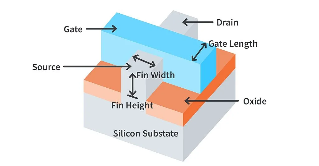
FinFET is built on a SOI (Silicon-on-insulator) or bulk silicon wafer that can be fabricated using an existing CMOS compatible technology. Like the conventional MOSFET transistor, FinFET also has a source, drain, and gate terminal to control the flow of current. What makes the FinFET differ from a MOSFET is the channel between the source and drain of FinFET. The channel on top of the silicon substrate is a three-dimensional bar, which is called a “fin”.
The three-dimensional 'fins' form the source and drain, enabling more volume than a planar transistor for the same area. The gate orientation is at a right angle to the vertical fin, traversing one side of the fin to the other; it wraps over the fin, enabling it to interface with three sides of the fin. This forms several gate electrodes on each side of the fin or channel which reduce current leakage effects and improve drive current.
In traditional MOS, a dopant is inserted into the channel, reducing SCEs and ensuring high threshold voltage. In FinFET, the gate structure is wrapped around the channel and the body is thin, also reducing SCEs and making channel doping optional. Therefore, FinFET suffers less from dopant-induced variations and low channel doping also ensures better mobility of the carriers inside the channel. This allows the use of lower threshold voltages and results in better performance and lower power dissipation.
Based on the design structure, the fin height of a single-fin FinFET must be half of the effective channel width (electrical width), Weff. The drive current of the FinFET can be increased by increasing the height of the fin, thereby increasing the width of the channel. Constructing multiple parallel fins as shown in Figure 2 provides higher drive current strengths per unit area. The Weff of FinFET is given by

where,
- NFIN is the number of fins aligned in parallel
- TFIN is the thickness (width), and
- HFIN is the height of each fin.
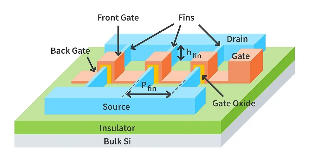
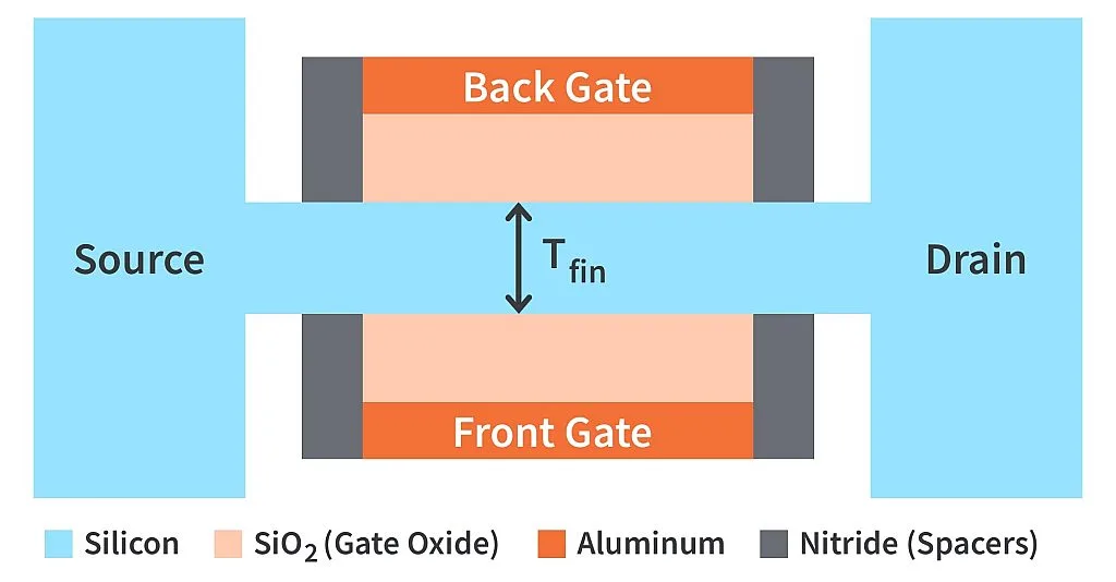
Figure 3 shows the material used for the different FinFET regions. Nitride spacers are used as gate insulators and the gate oxide is of SiO2 type. The front and back gate electrodes are of aluminium metal. The source and drain are homogenous having ohmic contact with aluminium electrodes. FinFETs exploit symmetric gates to achieve high performance, but can be fabricated with asymmetric gates to target threshold voltage.
Despite high fabrication costs, FinFET technology provides numerous advantages such as lower switching voltage, higher drive current for a given transistor footprint hence higher operating speed, lower leakage hence lower power consumption, no random dopant fluctuation hence better carrier mobility and scaling of the transistor in the nanoscale.
