The BJT is constructed with three doped semiconductor regions (emitter, base, and collector) separated by two pn junctions.
One type consists of two n regions separated by a p region (npn), and the other type consists of two p regions separated by an n region (pnp).
The term bipolar refers to the use of both holes and electrons as current carriers in the transistor structure.
Figure 1: Basic BJT structure
The pn junction joining the base region and the emitter region is called the base-emitter junction.
The pn junction joining the base region and the collector region is called the base-collector junction.
A wire lead connects to each of the three regions.
The leads are labeled E, B, and C for emitter, base, and collector, respectively.
The base region is lightly doped and very thin compared to the heavily doped emitter and the moderately doped collector regions.
Figure 2 shows the schematic symbols for the npn and pnp bipolar junction transistors.
Figure 2: Standard BJT symbols
Basic BJT Operation
Biasing
Figure 3 shows a bias arrangement for both npn and pnp BJTs for operation as an amplifier. In order for a BJT to operate properly, the two pn junctions must be correctly biased with external DC voltages.
Figure 3: Forward-reverse bias of a BJT
In both cases the base-emitter (BE) junction is forward-biased and the base-collector (BC) junction is reverse-biased. This condition is called forward-reverse bias.
Basic BJT Operation
Operation: Inside the npn structure
The heavily doped n-type emitter region has a very high density of conduction-band (free) electrons.
These free electrons easily diffuse through the forward-based BE junction into the lightly doped and very thin p-type base region.
The base has a low density of holes, which are the majority carriers.
A small percentage of the total number of free electrons injected into the base region recombine with holes and move as valence electrons through the base region and into the emitter region as hole current.
Figure 4: BJT operation showing electron flow
When the electrons that have recombined with holes leave the crystalline structure of the base, they become free electrons in the metallic base lead and produce the external base current.
As the free electrons move toward the reverse-biased BC junction, they are swept across into the collector region by the attraction of the positive collector supply voltage.
The free electrons move through the collector region, into the external circuit, then return into the emitter region along with the base current.
The emitter current is slightly greater than the collector current because of the small base current that splits off from the total current injected into the base region from the emitter.
The operation of the pnp is the same as for the npn except that the roles of the electrons and holes, the bias voltage polarities, and the current directions are all reversed.
Basic BJT Operation
Transistor Currents
The directions of the currents in both npn and pnp transistors and the schematic symbols are as shown in Figure 5.
Figure 5: Transistor currents
The arrow on the emitter inside the transistor symbols points in the direction of the conventional current.
These diagrams show that the emitter current (IE) is the sum of the collector current (IC) and the base current (IB), expressed as:
BJT Characteristics and Parameters
DC Beta (βDC) and DC Alpha (αDC)
The DC current gain of a transistor is the ratio of the DC IC to DC IB and is designated DC beta (βDC).
βDC is usually designated as an equivalent hybrid (h) parameter, hFE, on transistor datasheets: βDC= hFE.
The ratio of the DC IC to the DC IE is the dc alpha (αDC). The alpha is a less-used parameter than beta in transistor circuits.
BJT Characteristics and Parameters
Transistor DC Model
Fig. 6 shows the unsaturated BJT as a device with a current input and a dependent current source in the output circuit for an npn.
Figure 6: Ideal dc model of an npn transistor
The input circuit is a forward-biased diode through which there is base current.
The output circuit is a dependent current source (diamond-shaped element) with a value that is dependent on IB.
BJT Characteristics and Parameters
BJT Circuit Analysis
Consider the basic transistor bias circuit in Fig. 7.
Figure 7: Transistor currents and voltages
VBE: DC voltage at base with respect to emitter
VCB: DC voltage at collector with respect to base
VCE: DC voltage at collector with respect to emitter
VBB forward-biases the base-emitter junction, and VCC reverse-biases the base-collector junction. When the base-emitter junction is forward-biased,
Although VBE can be as high as 0.9 V in an actual transistor and is dependent on current, 0.7 V is used to simplify the analysis of the basic concepts.
The characteristic of the base-emitter junction is the same as a normal diode curve.
Since the emitter is at ground (0 V), by Kirchhoff’s voltage law, the voltage across RB is
By Ohm’s law, VRB=IBRB. Substituting for VRB and solving for IB,
The voltage at the collector with respect to the grounded emitter is
Since the drop across RC is VRC=ICRC, VCE can be written as
The voltage across the reverse-biased collector-base junction is
BJT Characteristics and Parameters
Collector Characteristic Curves
Using a circuit like that shown in Fig. 8, a set of collector characteristic curves can be generated that show how IC varies with VCE, for specified values of IB.
Figure 8: BJT circuit
Both VBB and VCC are variable sources of voltage. VBB is assumed to be set to produce a certain value of IB and VCC is zero. Thus, both the base-emitter junction and the base-collector junction are forward-biased because the base is at approximately 0.7 V while the emitter and the collector are at 0 V.
IB is through the base-emitter junction because of the low impedance path to ground and, therefore, IC is zero
Figure 9: Collector characteristic curves
When both junctions are forward-biased, the transistor is in the saturation region of operation. Saturation is the state of a BJT in which IC has reached a maximum and is independent of IB.
As VCC is increased, VCE increases as IC increases. This is the portion between points A and B in Fig. 9. IC increases as VCC is increased because VCE remains less than 0.7 V due to the forward-biased base-collector junction.
When VCE exceeds 0.7 V, the base-collector junction becomes reverse-biased and the transistor goes into the active, or linear, region of operation.
IC increases very slightly for a given IB as VCE increases due to widening of the base-collector depletion region. This causes a slight increase in βDC.
This is the portion between points B and C in Fig. 9. IC in this portion is determined only by IC =βDCIB.
When VCE reaches a sufficiently high voltage, the base-collector junction goes into breakdown; and IC increases rapidly, shown by the portion to the right of point C. A transistor should never be operated in this region.
A family of curves is produced when IC versus VCE is plotted for values of IB. When IB =0, the transistor is in the cutoff region. Cutoff is the nonconducting state of a transistor.
BJT Characteristics and Parameters
Cutoff
When IB=0, the transistor is in the cutoff region of its operation. This is shown in Fig. 10 with the base lead open, thus IB=0.
There is a very small amount of collector leakage current, ICEO, due mainly to thermally produced carriers.
ICEO will usually be neglected in circuit analysis so that VCE=VCC.
Base-emitter and base-collector junctions are reverse-biased. The subscript CEO represents collector-to-emitter with the base open.
Figure 10: Cutoff
BJT Characteristics and Parameters
Saturation
When the base-emitter junction becomes forward-biased and IB is increased, IC also increases and VCE decreases as a result of more drop across RC.
When VCE reaches its saturation value, VCE(sat), the base-collector junction becomes forward-biased and IC can increase no further. At the point of saturation, IC=βDCIB is no longer valid.
VCE(sat) for a transistor occurs somewhere below the knee of the collector curves, and it is usually only a few tenths of a volt.
Base-emitter and base-collector junctions are forward-biased.
Figure 11: Saturation
BJT Characteristics and Parameters
DC Load Line
Cutoff and saturation can be illustrated in relation to the collector characteristic curves by the use of a load line.
Figure 12: DC load line on a family of collector characteristic curves
The bottom of the load line is at ideal cutoff where IC=0 and VCE=VCC. The top of the load line is at saturation where IC=IC(sat) and VCE=VCE(sat).
In between cutoff and saturation along the load line is the active region of the transistor’s operation.
BJT Characteristics and Parameters
More About βDC
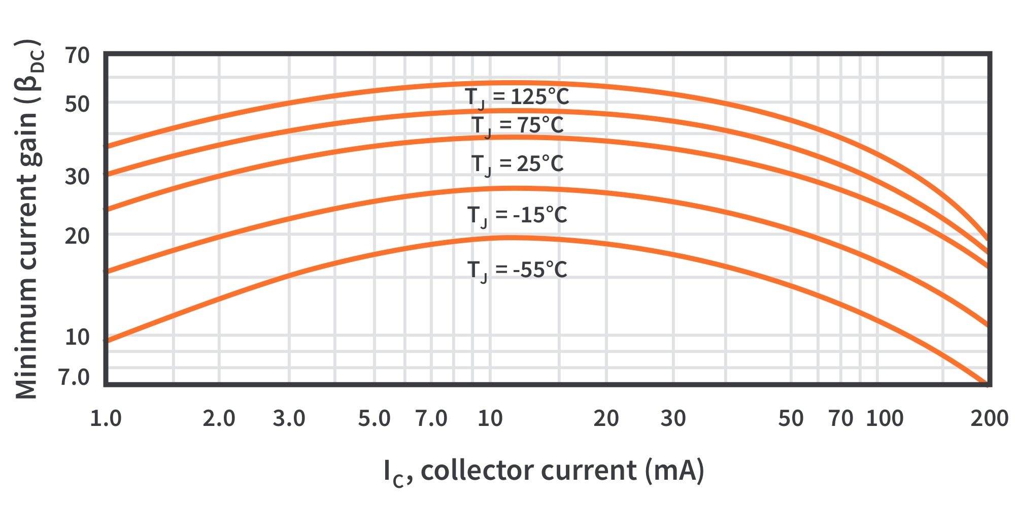
βDC varies with both IC and with temperature.
Keeping the junction temperature constant and increasing IC causes βDC to increase to a maximum.
A further increase in IC beyond maximum point causes βDC to decrease.
If IC is held constant and the temperature is varied, βDC changes directly with the temperature. If the temperature goes up, βDC goes up and vice versa.
Figure 13: Variation of DC beta with collector current for several temperatures
A transistor datasheet usually specifies βDC (hFE) at specific IC values. Even at fixed IC and temperature, βDC varies from one device to another for a given transistor due to unavoidable inconsistencies in manufacturing.
The βDC specified at a certain IC is usually the minimum value, βDC(min), although the maximum and typical values are sometimes specified.
BJT Characteristics and Parameters
Maximum Transistor Ratings
The product of VCE and IC must not exceed the maximum power dissipation PD(max). Both VCE and IC cannot be maximum at the same time. If VCE is maximum, IC can be calculated as
If IC is maximum, VCE can be calculated by
The BJT as an Amplifier
A transistor amplifies current because IC is equal to IB multiplied by the current gain, β.
IB is very small compared to IC and IE. Because of this,
An AC voltage, Vs, is superimposed on the DC bias voltage VBB as shown in Fig. 14. The DC bias voltage VCC is connected to the collector through RC.
Figure 14: Basic transistor amplifier circuit
Ib, Ic and Ie are the AC transistor currents. Vb, Vc and Ve are AC voltages from the transistor terminals to the ground.
The AC Vin produces an AC IB, which results in a much larger AC IC.
The AC IC produces an ac voltage across RC, producing an amplified, but inverted, reproduction of the ac input voltage in the active region of operation.
The forward-biased base-emitter junction presents a very low resistance to the ac signal. This internal AC emitter resistance (r'e) appears in series with RB. The AC base voltage is
The AC collector voltage, Vc, equals the AC voltage drop across RC: .
Since , the AC collector voltage is .
Vb can be considered the transistor AC input voltage where Vb =Vs-IbRB.
Vc can be considered the transistor AC output voltage.
Since voltage gain is defined as the ratio of the output voltage to the input voltage, the ratio of Vc to Vb is the AC voltage gain, Av, of the transistor.
Substituting IeRC for Vc and Ier'e for Vb,
The BJT as a Switch
Figure 15: Switching action of an ideal transistor
In Fig. 15(a), the transistor is in the cutoff region because the base-emitter junction is not forward-biased. There is, ideally, an open between collector and emitter.
In Fig. 15(b), the transistor is in the saturation region because the base-emitter junction and the base-collector junction are forward-biased. IB is made large enough to cause IC to reach its saturation value.
There is, ideally, a short between collector and emitter. A small voltage drop across the transistor of up to a few tenths of a volt normally occurs, which is the saturation voltage, VCE(sat).
Conditions in Cutoff
The base-emitter junction is not forward-biased. Neglecting leakage current, all of the currents are zero, and VCE=VCC,
Conditions in Saturation
The base-emitter junction is forward-biased and there is enough IB to produce a maximum IC. The collector saturation current is
Since VCE(sat) is very small compared to VCC, it can usually be neglected. The minimum value of IB needed to produce saturation is
Normally, IB should be significantly greater than IB(min) to ensure that the transistor is saturated.
Get the latest tools and tutorials, fresh from the toaster.


 .
. , the AC collector voltage is
  .
.


