Power amplifiers have the objective of delivering power to a load. This means that components must be considered in terms of their ability to dissipate heat.
The Class A Power Amplifier
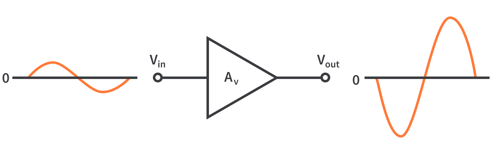
A class A amplifier is biased such that it always operates in the linear region where the output signal is an amplified replica of the input signal.
For a small-signal amplifier, the AC signal moves over a small percentage of the total AC load line.
For a large-signal amplifier, the output signal is larger and approaches the limits of the AC load line
Both large-signal and small-signal amplifiers are considered to be class A if they operate in the linear region at all times.
Figure 1: Class A amplifier operation. Output is shown 180° out of phase with the input
Heat Dissipation
Power devices must dissipate a large amount of internally generated heat.
For BJT power transistors, the collector terminal is the critical junction:
The transistor’s case is always connected to the collector terminal. The case is designed to provide a large contact area between it and an external heat sink.
Heat from the transistor flows through the case to the heat sink and then dissipates in the surrounding air.
Heat sinks vary in size, number of fins, and type of material. Their size depends on the heat dissipation requirement and the maximum ambient temperature of transistor operation.
Centered Q-Point
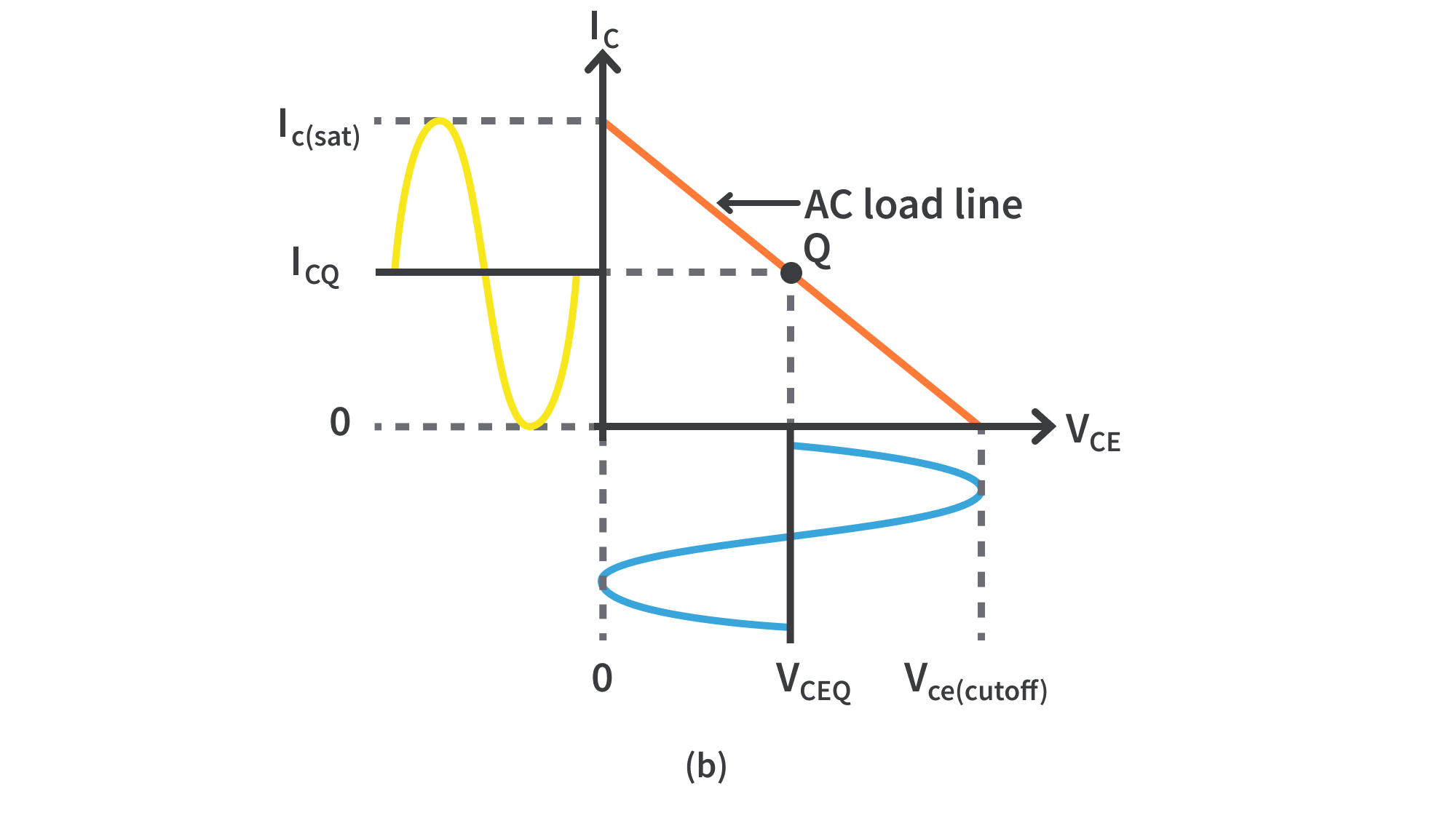
DC and AC load lines intersect at the Q-point. When the Q-point is at the center of the AC load line, the maximum class A signal can be obtained.
Figure 2: Maximum class A output occurs when the Q-point is centered on the AC load line
This graph shows the AC load line with the Q-point at its center. IC can vary from its Q-point value, ICQ, up to its saturation value, Ic(sat), and down to its cutoff value of zero.
VCE can swing from its Q-point value, VCEQ, up to its cutoff value, Vce(cutoff), and down to its saturation value of near zero.
This operation is indicated in Fig. 2(b). The peak value of IC equals ICQ, and the peak value of VCE equals VCEQ in this case.
This signal is the maximum that can be obtained from the class A amplifier.
Figure 3: Q-point closer to cutoff
Fig. 3 shows an AC load line with the Q-point not centered and moved away from center toward cutoff. The output variation is limited by cutoff in this case.
IC can only swing down to near zero and an equal amount above ICQ . VCE can only swing up to its cutoff value and an equal amount below VCEQ.
This situation is illustrated in Fig. 3(a). If the amplifier is driven any further than this, it will “clip” at cutoff, as shown in Fig. 3(b).
Figure 4: Q-point closer to saturation
Fig. 4 shows an AC load line with the Q-point moved away from center toward saturation. The output variation is limited by saturation.
IC can only swing up to near saturation and an equal amount below ICQ. VCE can only swing down to its saturation value and an equal amount above VCEQ.
This situation is illustrated in Fig. 4(a). If the amplifier is driven any further, it will “clip” at saturation, as shown in Fig. 4(b).
Power Gain
The power gain of an amplifier is the ratio of the output power (power delivered to the load) to the input power. In general, power gain is
where Ap is the power gain, PL is signal power delivered to the load, and Pin is signal power delivered to the amplifier.
The power gain can be computed by any of several formulas, depending on what is known.
Frequently, the easiest way to obtain power gain is from input resistance, load resistance, and voltage gain:
Since VL/Vin = Av ,
The formula can be applied to any amplifier.
For a common-collector (CC) amplifier, Ap is just the ratio of the input resistance to the output load resistance.
DC Quiescent Power
The power dissipation of a transistor with no signal input is the product of its Q-point current and voltage.
The DC quiescent power is the maximum power that a class A amplifier can handle. The transistor’s power rating must exceed this value.
Output Power
In general, the output signal power is the product of the RMS load current and the RMS load voltage.
The maximum unclipped AC signal occurs when the Q-point is centered on the AC load line. For a CE amplifier with a centered Q-point, the maximum peak voltage swing is
The RMS value is 0.707Vc(max).
The maximum peak current swing is
The RMS value is 0.707Ic(max).
The maximum power out from a class A amplifier is
Efficiency
The efficiency of any amplifier is the ratio of the output signal power supplied to a load to the total power from the DC supply.
The average power supply current, ICC, is equal to ICQ and the supply voltage is at least 2VCEQ. Therefore, the total DC power is
The maximum efficiency, nmax, of a capacitively coupled class A amplifier is
The maximum efficiency of a capacitively coupled class A amplifier cannot be higher than 0.25, or 25%, and, in practice, is usually considerably less (~10%).
In general, the low efficiency of class A amplifiers limits their usefulness to low power applications that usually require less than 1 W.
The Class B and Class AB Push-Pull Amplifiers
A class B amplifier is biased at cutoff so that it operates in the linear region for 180⁰ of the input cycle and is in cutoff for 180⁰.
Class AB amplifiers are biased to conduct for slightly more than 180⁰.
Class B Operation
The class B operation is illustrated in Fig. 5, where the output waveform is shown relative to the input in terms of time (t).
Figure 5: Basic class B amplifier operation (noninverting)
The Q-Point Is at Cutoff
The class B amplifier is biased at the cutoff point so that ICQ =0, VCEQ=VCE(cutoff).
It is brought out of cutoff and operates in its linear region when the input signal drives the transistor into conduction. This is illustrated in Fig. 6 with an emitter-follower circuit where the output is not a replica of the input.
Figure 6: Common-collector class B amplifier
Class B Push-Pull Operation
The combination of two class B amplifiers working together is called push-pull operation.
To amplify the entire cycle in Fig. 6, it is necessary to add a second class B amplifier that operates on the negative half.
There are two common approaches for using push-pull amplifiers:
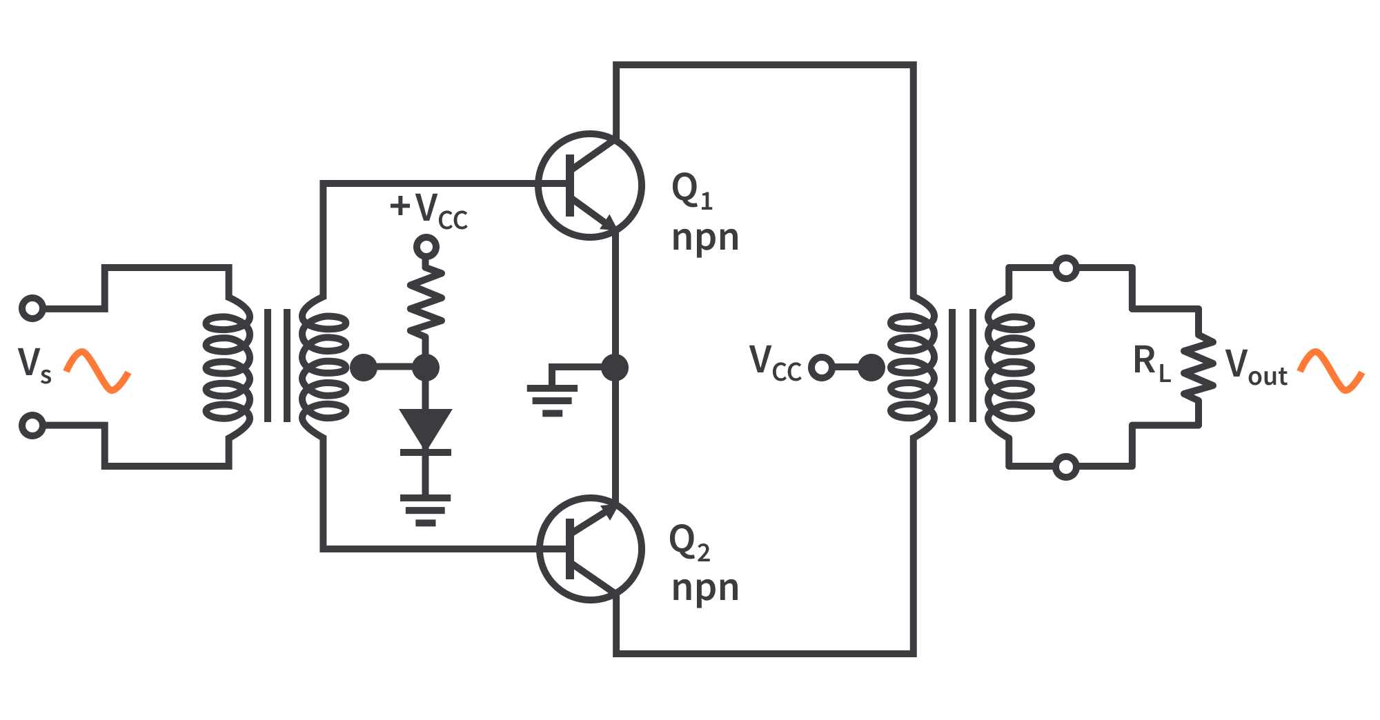
via transformer coupling
via complementary symmetry transistors; a matching pair of npn/pnp BJTs
The input transformer has a center-tapped secondary that is connected to ground, producing phase inversion of one side with respect to the other. This converts the input signal to two out-of-phase signals for the transistors.
Q1 conducts during the positive half-cycle; Q2 conducts during the negative half-cycle.
The output transformer permits current in both directions, combining the signals even though one transistor is always cut off. The positive power supply signal is connected to the center tap of the output transformer.
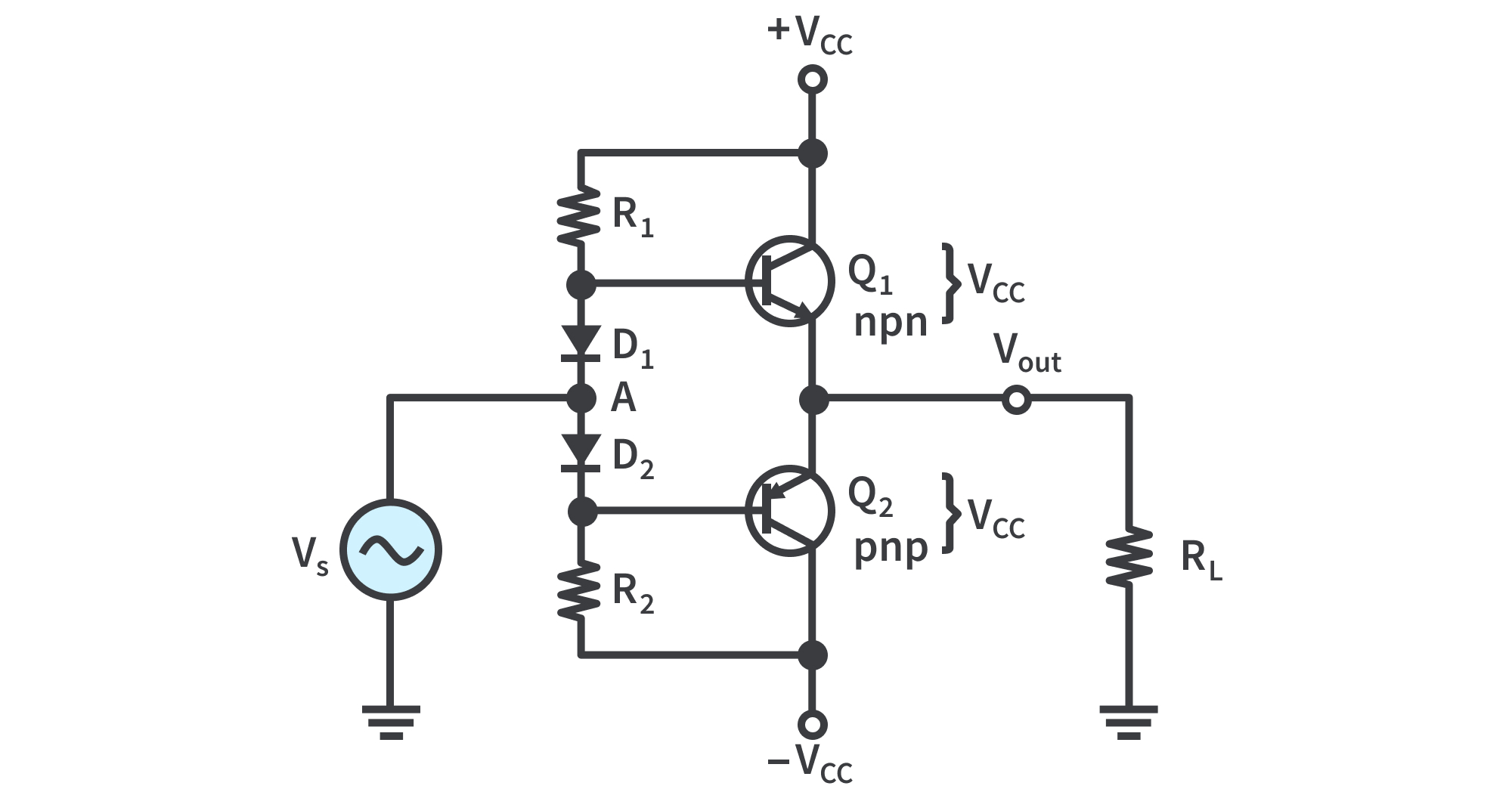
Complementary Symmetry Transistors
Figure 8: Class B push-pull AC operation
Fig. 8 uses two emitter-followers and both positive and negative power supplies.
One emitter-follower uses an npn transistor and the other a pnp, which conduct on opposite alternations of the input cycle. Notice that there is no DC base bias voltage (VB=0).
Only the signal voltage drives the transistor conduction. Q1 conducts during the positive half of the input cycle, and Q2 conducts during the negative half.
Crossover Distortion: When VB=0, both transistors are off and the input signal voltage must exceed VBE before a transistor conducts.
There is a time interval between the positive and negative alternations of the input when neither transistor is conducting, as shown in Fig. 9. The result is called crossover distortion.
Figure 9: Crossover distortion in a class B push-pull amplifier
Biasing the Push-Pull Amplifier for Class AB Operation
To overcome crossover distortion, the biasing is adjusted to just overcome the VBE of the transistors; this results in a modified form of operation called class AB.
In class AB operation, the push-pull stages are biased into slight conduction, even when no input signal is present. This can be done as shown in Fig. 10.
Figure 10: Biasing the push-pull amplifier with current-mirror diode bias to eliminate crossover distortion.. The transistors form a complementary pair (one npn and one pnp).
Current mirror: when the diode characteristics of D1 and D2 are closely matched to that of the transistor base-emitter junctions, the current in the diodes and in the transistors are the same.
In the bias path of the circuit, R1 and R2 are of equal value, as are the + /- supply voltages, forcing the voltage at point A to be 0 V and eliminating the need for an input coupling capacitor.
The DC voltage on the output is also 0 V. Assuming that both diodes and both complementary transistors are identical, the drop across D1 equals the VBE of Q1, and the drop across D2 equals the VBE of Q2.
The DC voltage on the output is also 0 V.
Assuming that D1, D2, and both transistors are identical, VD1= VBE of Q1, and VD2 = VBE of Q2. Since they are matched, the diode current will be the same as ICQ.
The diode current and ICQ can be found by applying Ohm’s law to either R1 or R2 as follows:
Crossover distortion also occurs in transformer-coupled amplifiers. In this case, 0.7 V is applied to the input transformer’s secondary that just biases both transistors into conduction.
The bias voltage to produce this drop can be derived from the power supply using a single diode as shown in Fig. 11.
Figure 11: Eliminating crossover distortion in a transformer-coupled push-pull amplifier. The biased diode compensates for the base-emitter drop of the transistors and produces class AB operation.
AC Operation
Consider the AC load line for Q1 in Fig. 10. The Q-point is slightly above cutoff. The AC cutoff voltage for a two-supply operation is at VCC with an ICQ as given earlier.
Ic(sat) for a two-supply operation with a push-pull amplifier is
The AC load line for the npn transistor is as shown in Fig 12. The DC load line can be found by drawing a line that passes through VCEQ and Ic(sat).
Figure 12: Load lines for a complementary symmetry push-pull amplifier. Only the load lines for the npn transistor are shown.
The saturation current for DC is the current if the collector to emitter is shorted on both transistors.
This assumed short across the power supplies obviously would cause maximum current from the supplies and implies the DC load line passes almost vertically through the cutoff.
Operation along the DC load line, such as caused by thermal runaway, could produce such a high current that the transistors are destroyed.
Fig. 13(a) illustrates the AC load line for Q1 in Fig. 13(b).
Figure 13: AC load line for Q1
In this case, a signal is applied that swings over the region of the AC load line shown in bold.
At the upper end of the AC load line, the voltage across the transistor (Vce) is a minimum, and the output voltage is maximum.
Single-Supply Push-Pull Amplifier
Push-pull amplifiers using complementary symmetry transistors can be operated from a single voltage source as shown in Fig. 14.
Figure 14: Single-ended push-pull amplifier
The circuit operation is the same, except the bias is set to force the output emitter voltage to be VCC/2 instead of 0 V.
Capacitive coupling for the input and output is necessary to block the bias voltage from the source and the load resistor.
Ideally, the output voltage can swing from zero to VCC, but in practice it does not quite reach these ideal values.
Class B/AB Power
Maximum Output Power
The ideal maximum peak output current for both dual-supply and single-supply push-pull amplifiers is approximately Ic(sat), and the maximum peak output voltage is approximately VCEQ.
Since Iout(rms) = 0.707Ic(sat) and Vout(rms) = 0.707VCEQ , Pout = 0.5Ic(sat)VCEQ. Substituting VCEQ = VCC/2, the maximum average output power is
DC Input Power
The DC input power comes from the VCC supply and is PDC = ICCVCC. Since each transistor draws current for a half-cycle, the current is a half-wave signal with an average value of . So
Efficiency
An advantage of push-pull class B and class AB amplifiers over class A is a much higher efficiency.
This advantage usually overrides the difficulty of biasing the class AB push-pull amplifier to eliminate crossover distortion.
Recall: . The maximum efficiency for a class B amplifier (class AB is slightly less) is calculated as
Input Resistance
The complementary push-pull configuration used in class B/AB amplifiers is, in effect, two emitter-followers.
The input resistance for the emitter-follower, where R1 and R2 are the bias resistors is . Since RE = RL ,
The Class C Amplifier
Class C amplifiers are biased so that conduction occurs for much less than 180°.
Class C amplifiers are more efficient than either class A or push-pull class B and class AB; more output power can be obtained from class C operation.
The output amplitude is a nonlinear function of the input, so class C amplifiers are not used for linear amplification.
They are generally used in radio frequency (RF) applications, such as oscillators that have a constant output amplitude, and modulators, where a high-frequency signal is controlled by a low-frequency signal.
Basic Class C Operation
The basic concept of class C operation is illustrated in Fig. 15.
Figure 15: Basic class C amplifier operation (noninverting)
A common-emitter class C amplifier with a resistive load is shown in Fig. 16(a). It is biased below cutoff with the negative VBB supply.
The AC source voltage has a peak value that is slightly greater than |VBB|+VBE so that the base voltage exceeds the base-emitter barrier potential for a short time near the positive peak of each cycle, as shown in Fig. 16(b).
During this short interval, the transistor is turned on.
When the entire AC load line is used, as shown in Fig. 16(c), the ideal maximum collector current is Ic(sat), and the ideal minimum collector voltage is Vce(sat).
Figure 16: Basic class C operation
Power Dissipation
The power dissipation of the transistor in a class C amplifier is low because it is on for only a small percentage of the input cycle.
Fig. 17(a) shows the collector current pulses. The time between the pulses is the period (T ) of the AC input voltage. The collector current and the collector voltage during the on time of the transistor are shown in Fig.17(b).
Figure 17: Class C waveforms
Assume ideal pulse approximations.
If the output swings over the entire load, the maximum current amplitude is Ic(sat) and the minimum voltage amplitude is Vce(sat) during the time the transistor is on. The power dissipation during the on time is, therefore, .
The transistor is on for a short time, ton, and off for the rest of the input cycle. Assuming the entire load line is used, the power dissipation averaged over the entire cycle is
Maximum Output Power
Since the voltage developed across the tank circuit has a peak-to-peak value of approximately 2VCC, the maximum output power can be expressed as
Rc is the equivalent parallel resistance of the collector tank circuit at resonance and is the parallel combination of the coil resistance and the load resistance. The total power that must be supplied to the amplifier is
The efficiency is
When the class C efficiency approaches 1 (100%).
Clamper Bias for a Class C Amplifier
Fig. 18 shows a class C amplifier with a base bias clamping circuit. The base-emitter junction functions as a diode.
Figure 18: Class C amplifier with clamper bias
When the input signal goes positive, C1 is charged to the peak value with the polarity shown in Fig. 19(a). This action produces an average voltage at the base of approximately -Vp.
This places the transistor in cutoff except at the positive peaks, when the transistor conducts for a short interval.
For good clamping action, the R1C1 time constant of the clamping circuit must be much greater than the period of the input signal.
During the time up to the positive peak of the input (t0 to t1), the capacitor charges to Vp - 0.7V through the base-emitter diode, as shown in Fig.19(b).
During the time from t1 to t2, as shown in Fig.19(c), the capacitor discharges very little because of the large RC time constant. t. The capacitor maintains an average charge slightly less than Vp - 0.7V.
Figure 19: Clamper bias action
Since the DC input signal is zero (positive side of C1), the DC voltage at the base (negative side of C1) is slightly more positive than -(Vp-0.7V) as indicated in Fig.19(d).
As shown in Fig.19(e), the capacitor couples the AC input signal through to the base so that the voltage at the transistor’s base is the AC signal riding on a DC level slightly more positive than -(Vp-0.7V).
Near the positive peaks of the input voltage, the base voltage goes slightly above 0.7 V and causes the transistor to conduct for a short time, as shown in Fig.19(f).
CircuitBread is the best way to learn electronics.
Get the latest tools and tutorials, fresh from the toaster.


 . So
. So . The maximum efficiency for a class B amplifier (class AB is slightly less) is calculated as
  . Since RE = RL ,
 .
. the class C efficiency approaches 1 (100%).


