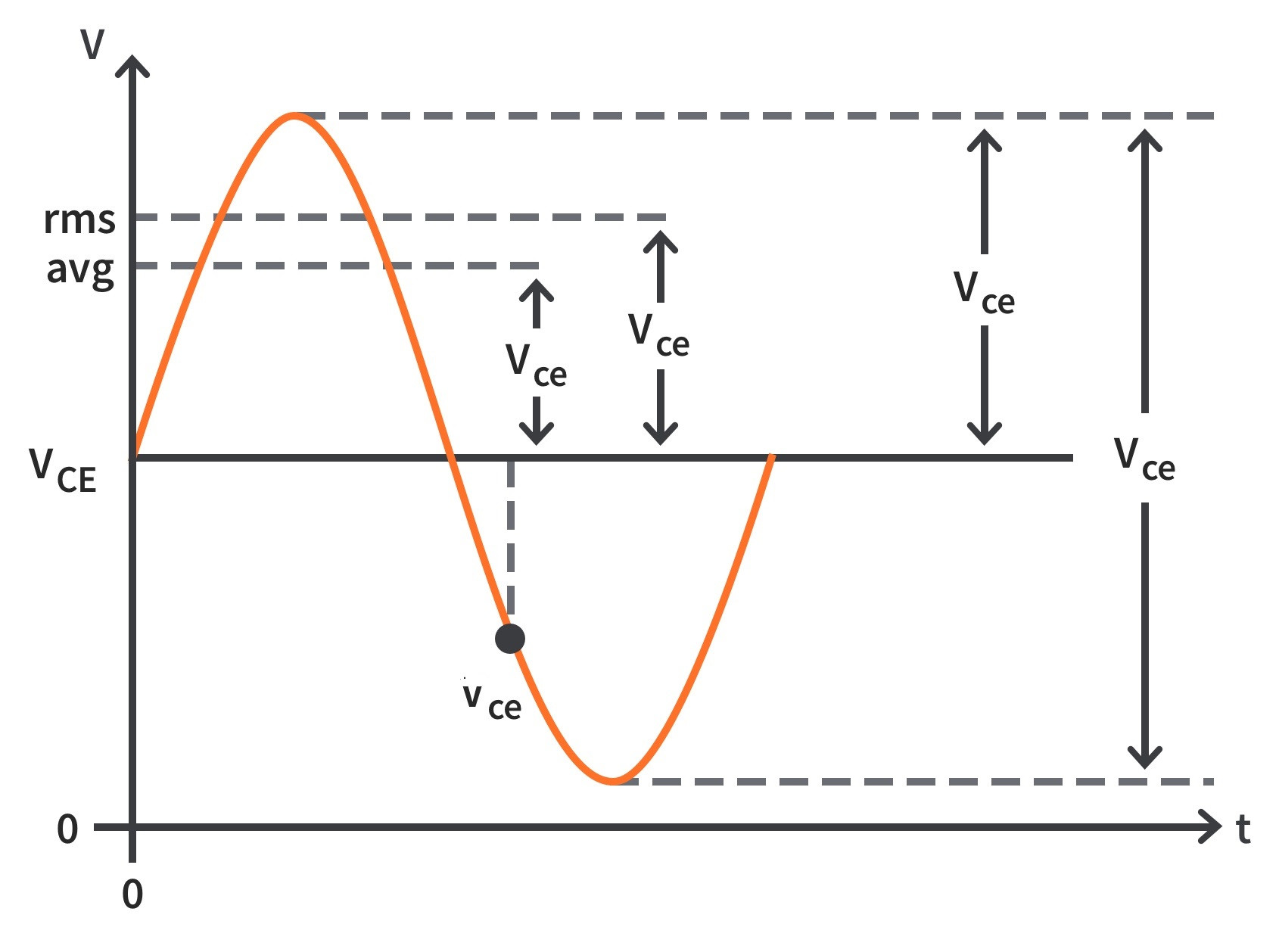
Lowercase italic subscripts are used to indicate ac quantities of rms, peak, and peak-to-peak currents and voltages: Ic , Ie , Ib , Vcand Vce (rms values are assumed unless otherwise stated).
Instantaneous quantities are represented by both lowercase letters and subscripts such as ic, ie, ib, and vce. For a specific voltage waveform,
Figure 1: Vce can be rms, average, peak, or peak-to-peak, but rms will be assumed unless stated otherwise. vce can be any instantaneous value on the curve.
Resistances often have different values when a circuit is analyzed from an AC viewpoint as opposed to a DC viewpoint. Lowercase subscripts are used to identify ac resistance values.
Resistance values internal to the transistor use a lowercase r' to show it is an AC resistance. An example is the internal ac emitter resistance, r'e.
The Linear Amplifier
A linear amplifier provides amplification of a signal without any distortion so that the output signal is an exact amplified replica of the input signal.
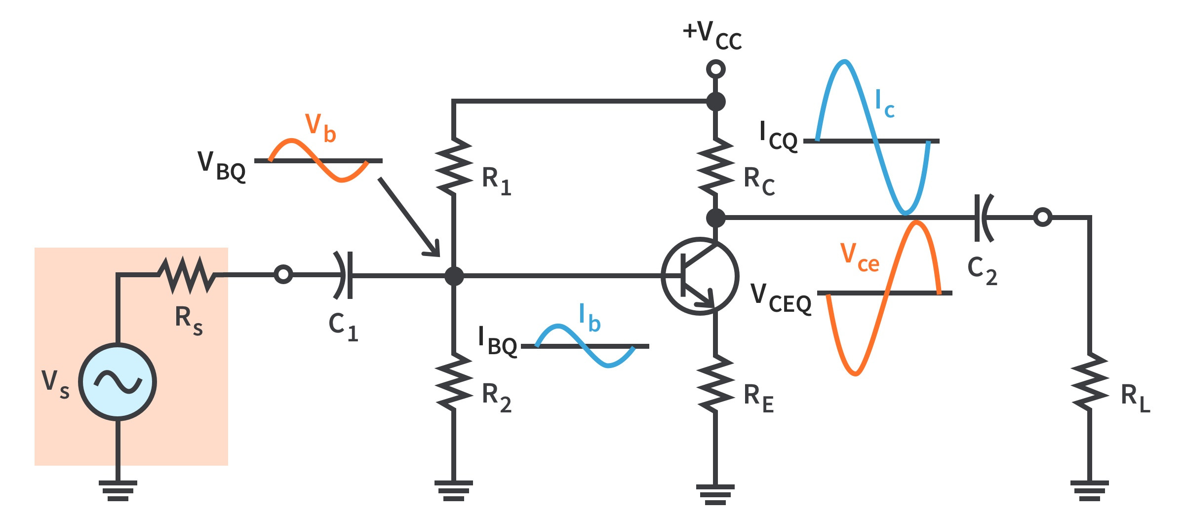
A transistor with a sinusoidal ac source capacitively coupled to the base through C1 and a load capacitively coupled to the collector through C2 is shown in Fig. 2.
Figure 2: An amplifier with voltage-divider bias driven by an ac voltage source with an internal resistance, Rs
The coupling capacitors block DC and thus prevent Rs and RL from changing the DC bias voltages at the base and collector.
The capacitors ideally appear as shorts to the signal voltage. Vs causes Vb to vary sinusoidally above and below its DC bias level, VBQ. The resulting variation in Ib produces a larger variation in Ic because of the current gain of the transistor.
As Ic increases, the collector voltage decreases. Ic varies above and below its Q-point value, ICQ, in phase with Ib.
Vce varies above and below its Q-point value, VCEQ, out of phase with Vb. A transistor always produces a phase inversion between the base voltage and the collector voltage.
Transistor AC Models
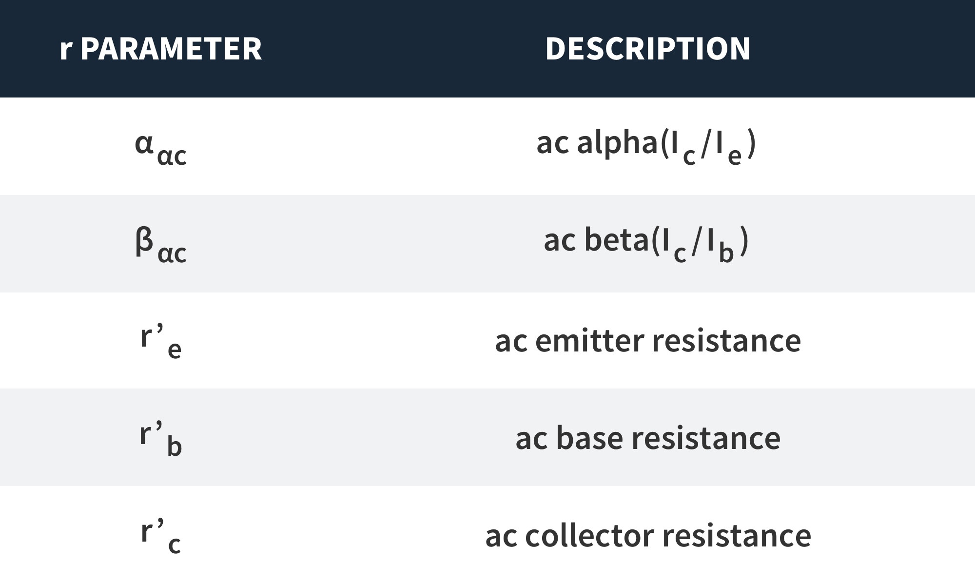
r Parameters
Figure 3: Commonly used r parameters for BJTs
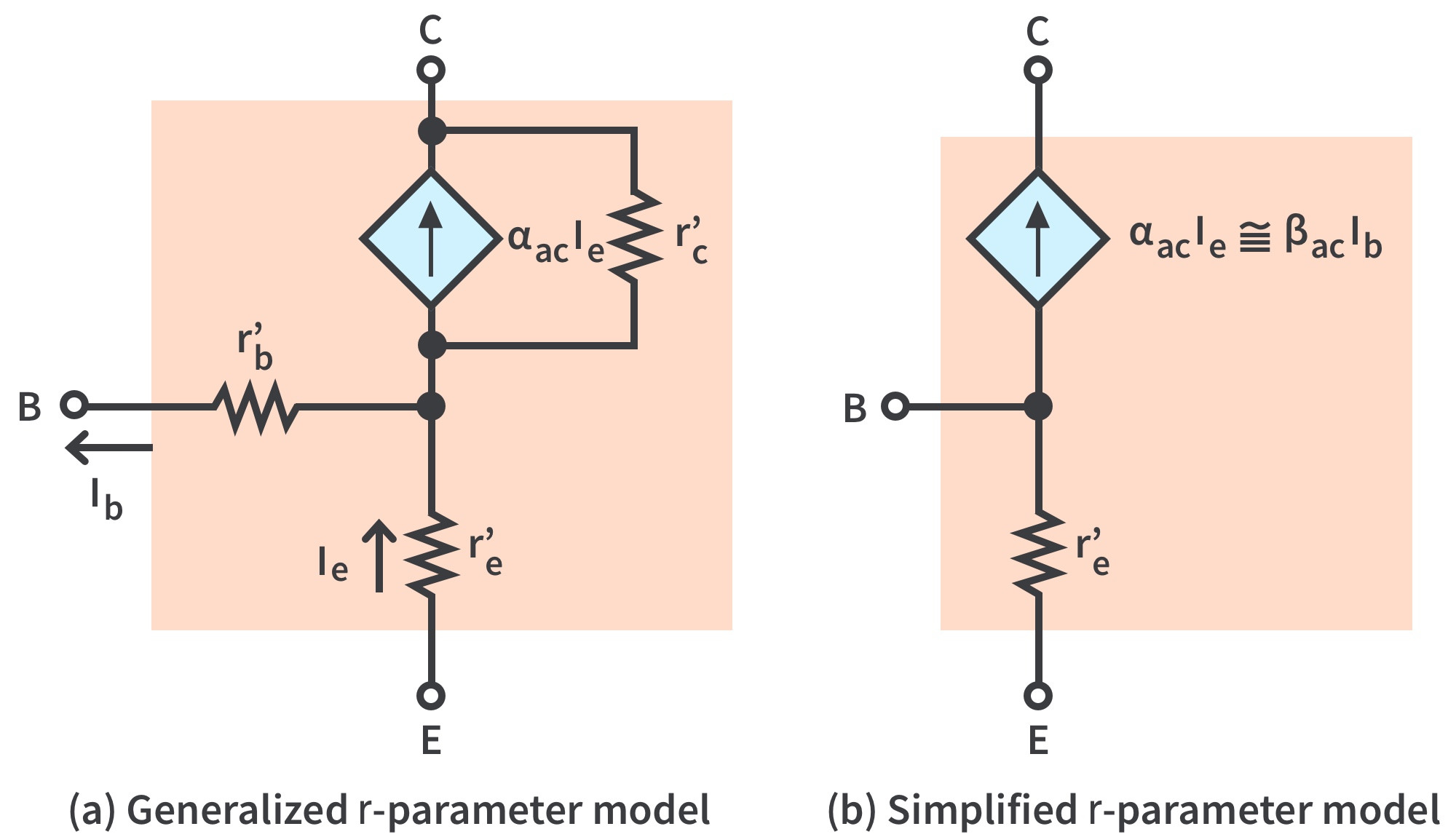
r Parameter Transistor Model
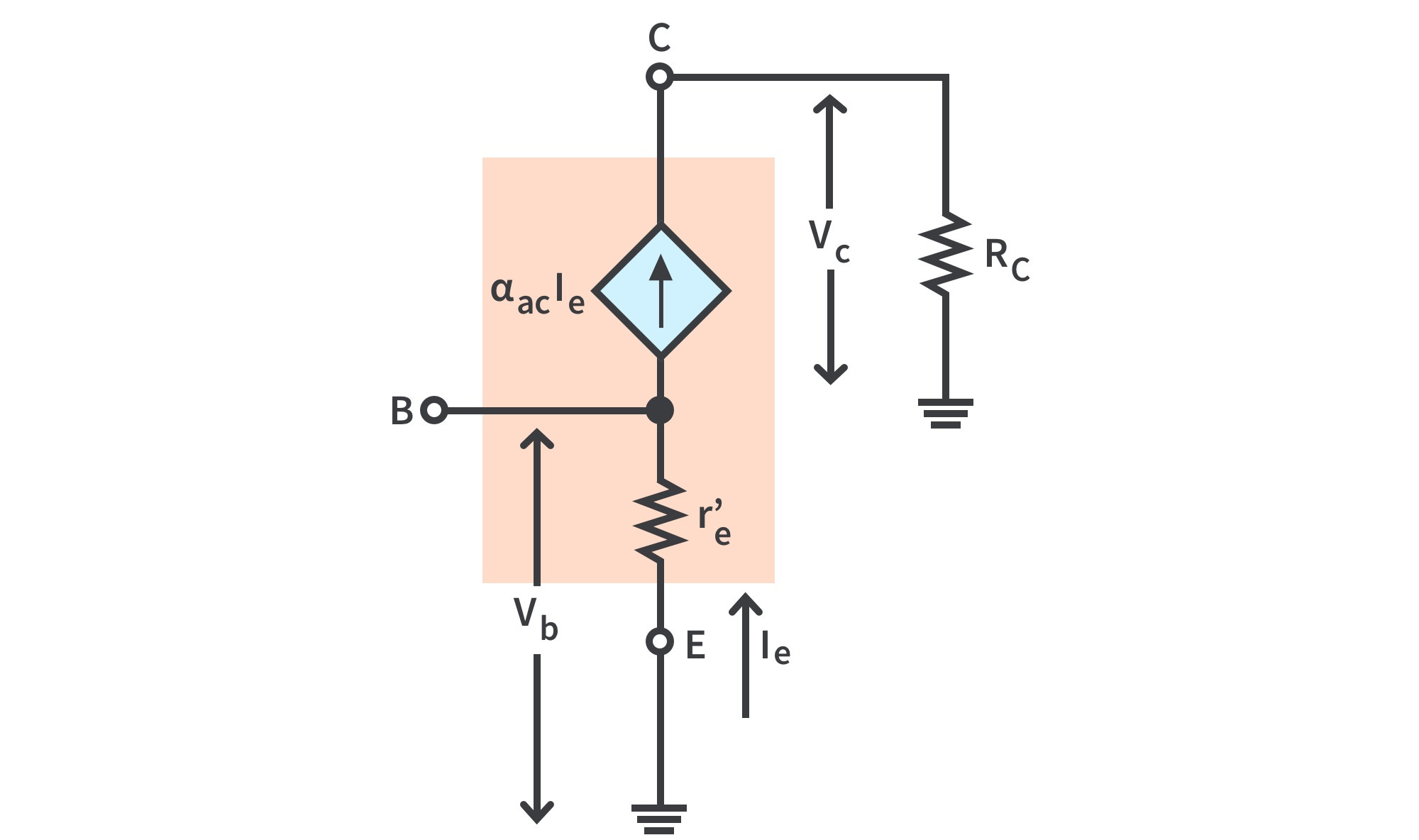
Figure 4: r-parameter transistor model
The effect of the AC base resistance rb' is usually small enough to neglect, so it can be replaced by a short.
The AC collector resistance rc' is usually several hundred kilohms and can be replaced by an open.
The resulting simplified r-parameter equivalent circuit is shown in Fig. 4(b).
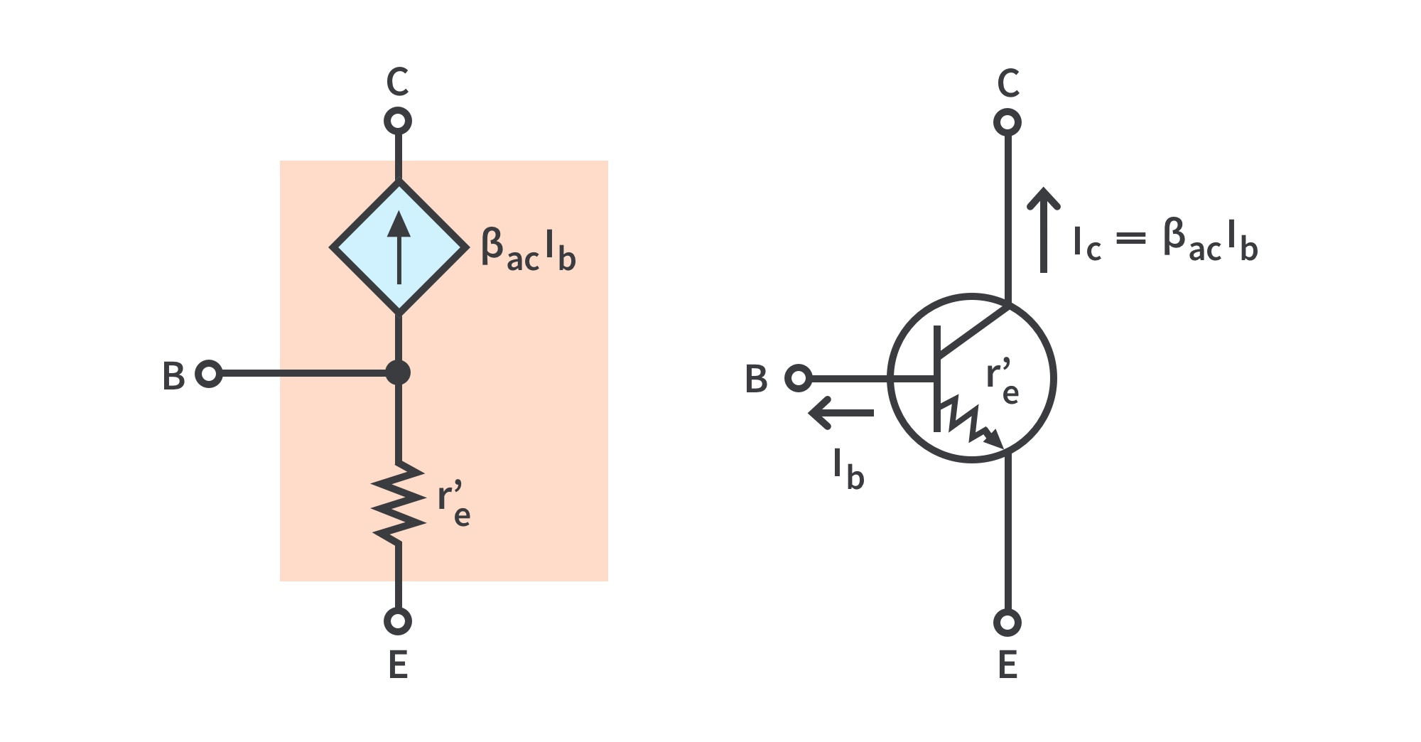
Figure 5: Relation of transistor symbol to r-parameter model
Transistor AC operation: A resistance appears between the emitter and base terminals. This is the resistance “seen” looking into the emitter for a forward-biased transistor.
The collector acts as a dependent current source of αacIe or, equivalently, βacIb(diamond-shaped symbol). These are shown with a transistor symbol in Fig. 5.
Determining re' by a Formula
The AC emitter resistance, re' is the most important of the r parameters for amplifier analysis.
For the approximate value of re', you can use
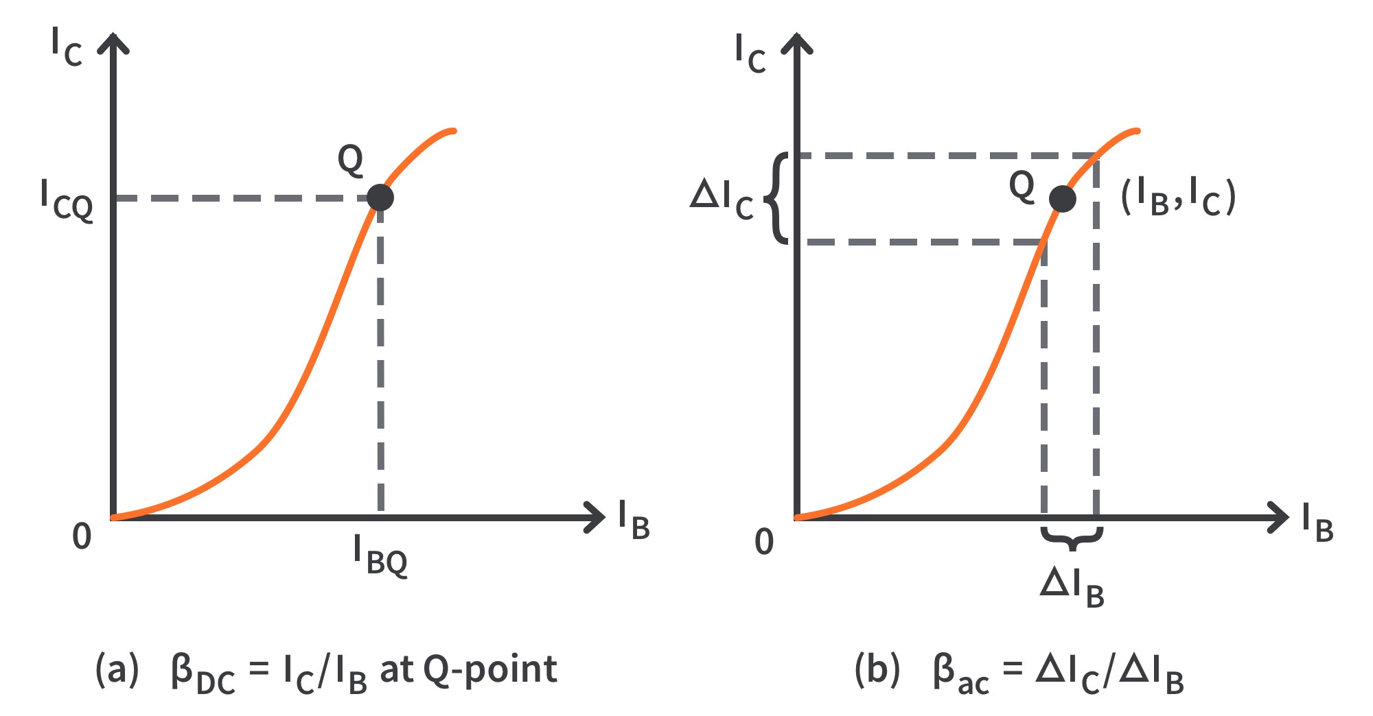
Comparison of the AC Beta (βac) to the DC Beta (βDC)
Figure 6: Difference between βac and βDC
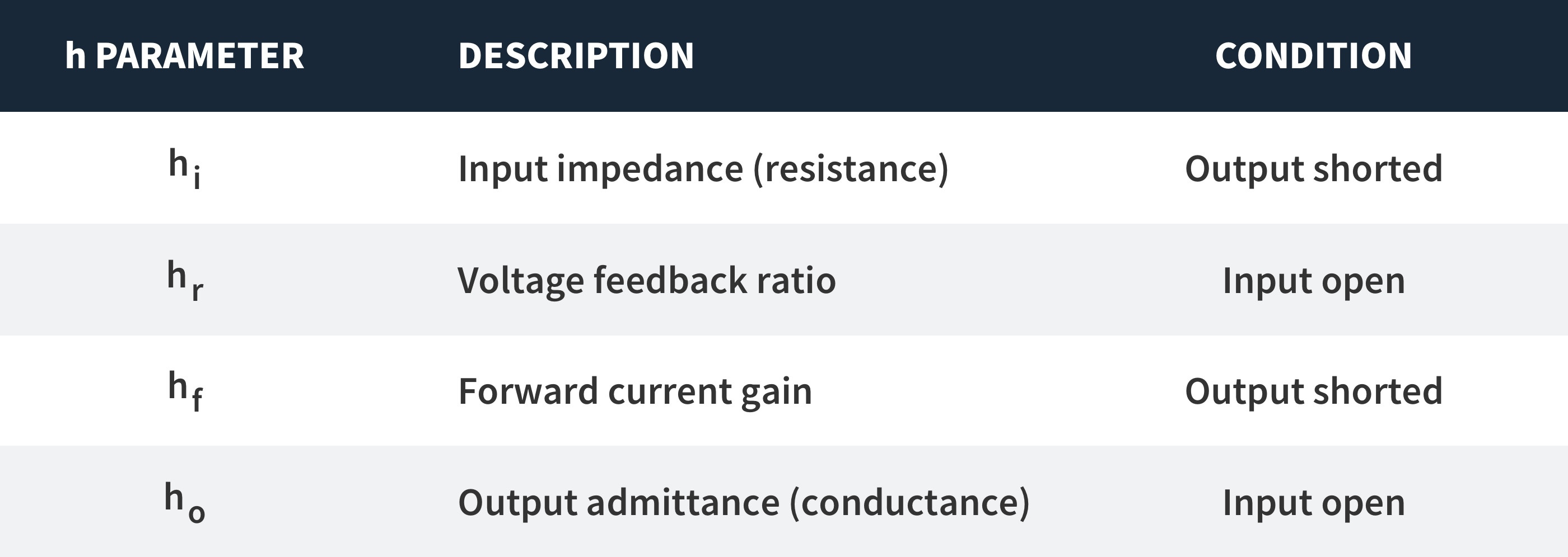
h Parameters
Figure 7: Basic ac h parameters
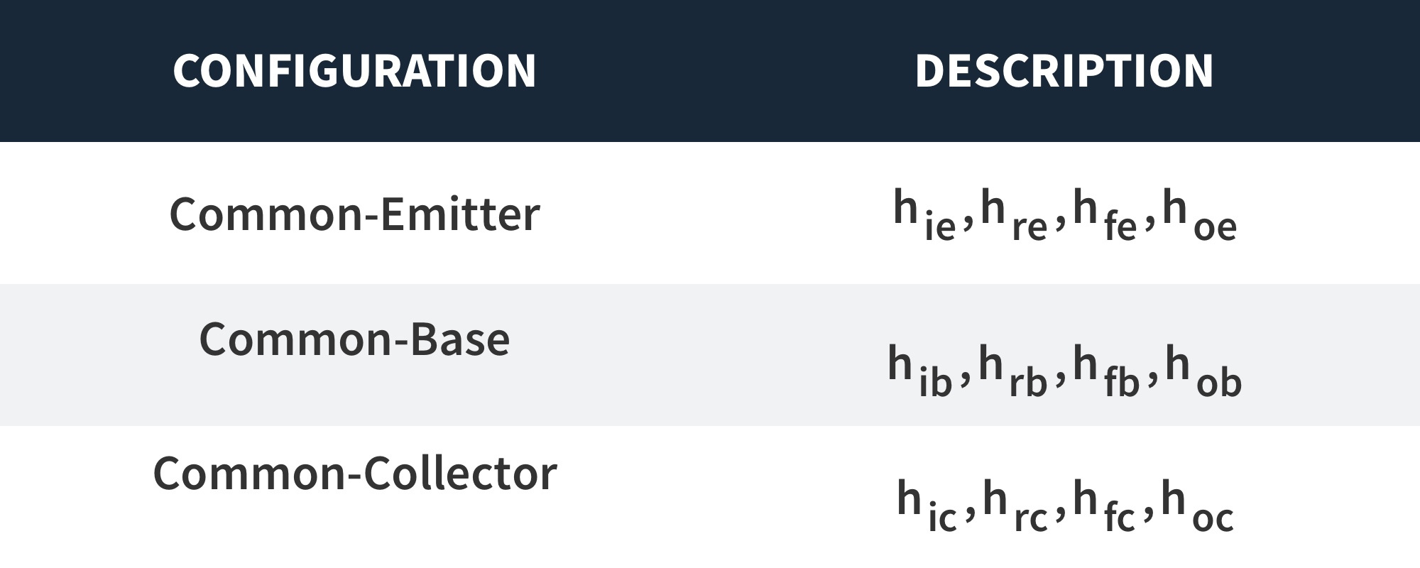
The four basic AC h parameters are hi, hr, hf and ho. Each of the parameters carries a second subscript to designate the common-emitter (e), common-base (b), or common-collector (c) amplifier configuration.
Figure 8: Subscripts of h parameters for each amplifier configuration
The term common refers to one of the three terminals (E, B, or C) that is referenced to AC ground for both input and output signals.
Relationships of h Parameters and r Parameters
Current ratios αac and βac convert directly from h parameters as follows:
Datasheets often provide only common-emitter h parameters. The following formulas show how to convert them to r parameters:
The Common-Emitter Amplifier
The common-emitter (CE) configuration has the emitter as the common terminal, or ground, to an AC signal.
CE amplifiers exhibit high voltage gain and high current gain.
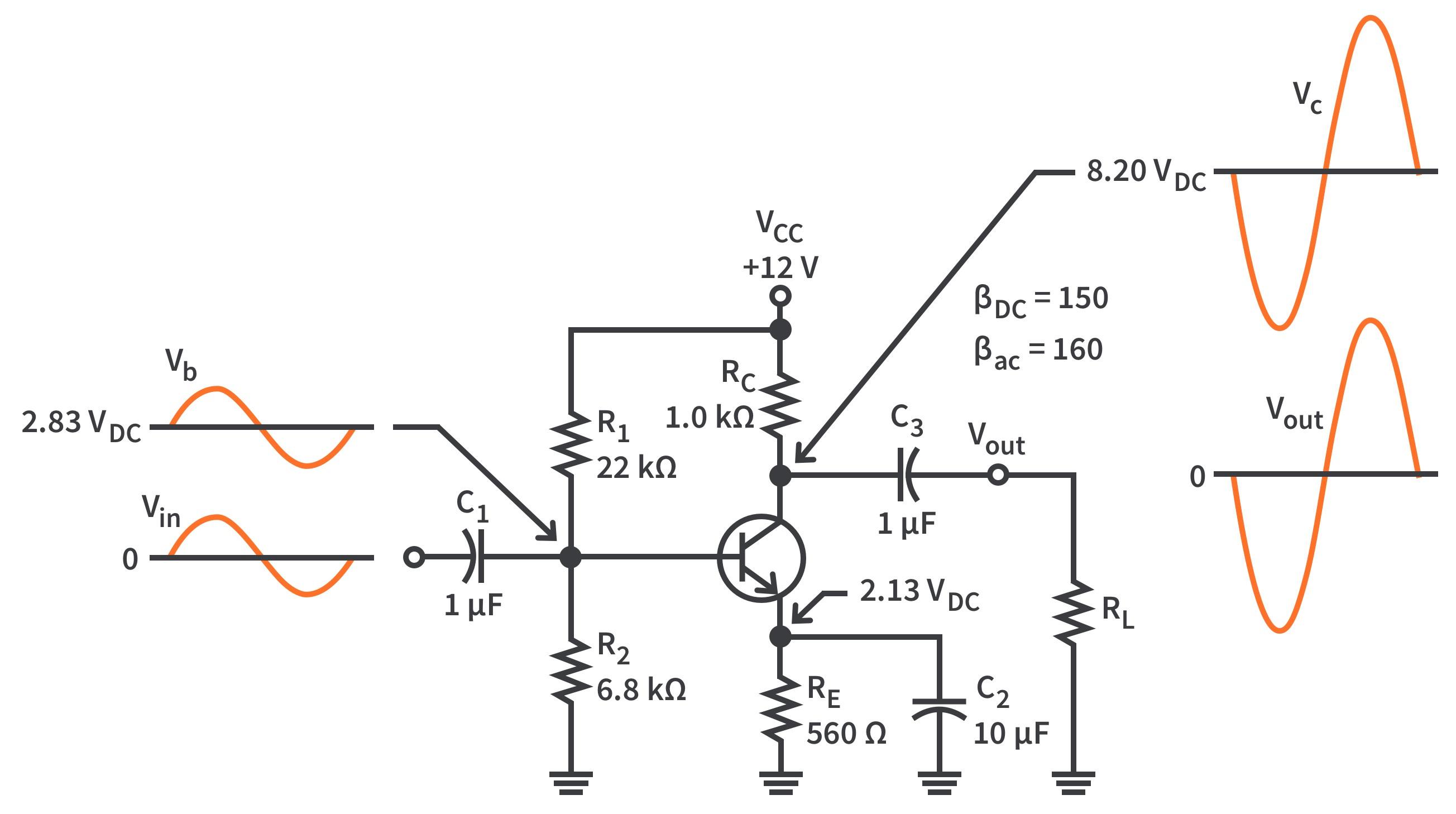
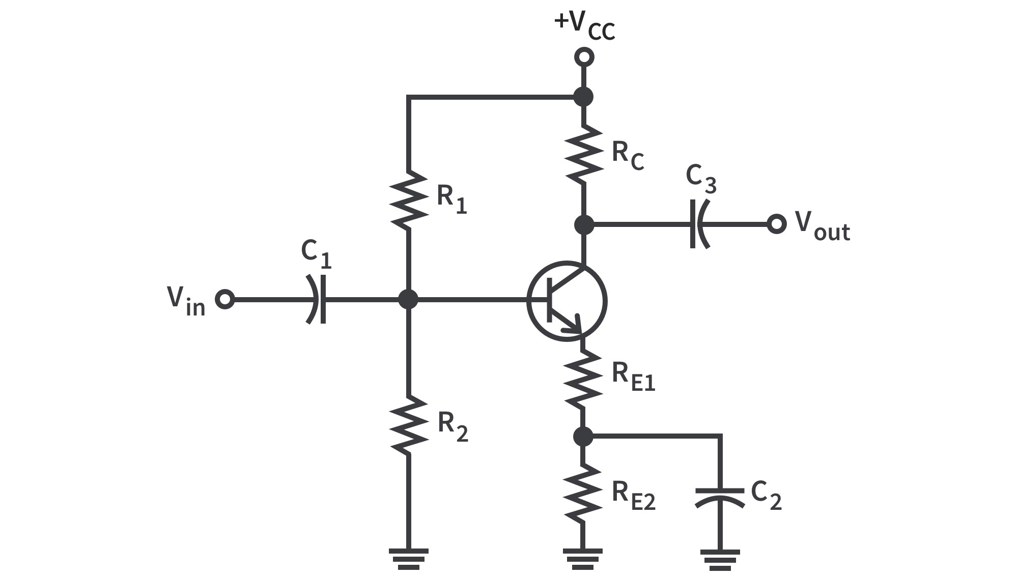
Fig. 9 shows a CE amplifier with voltage-divider bias and coupling capacitors C1 and C3, and a bypass capacitor, C2. Vin is capacitively coupled to the base terminal and Vout is capacitively coupled from the collector to the load.
The amplified output is 180° out of phase with the input.
Figure 9. A common-emitter amplifier
Since the AC signal is applied to the base as the input and taken from the collector as the output, the emitter is common to both the input and output signals.
There is no signal at the emitter because C2 shorts the emitter to the ground at the signal frequency.
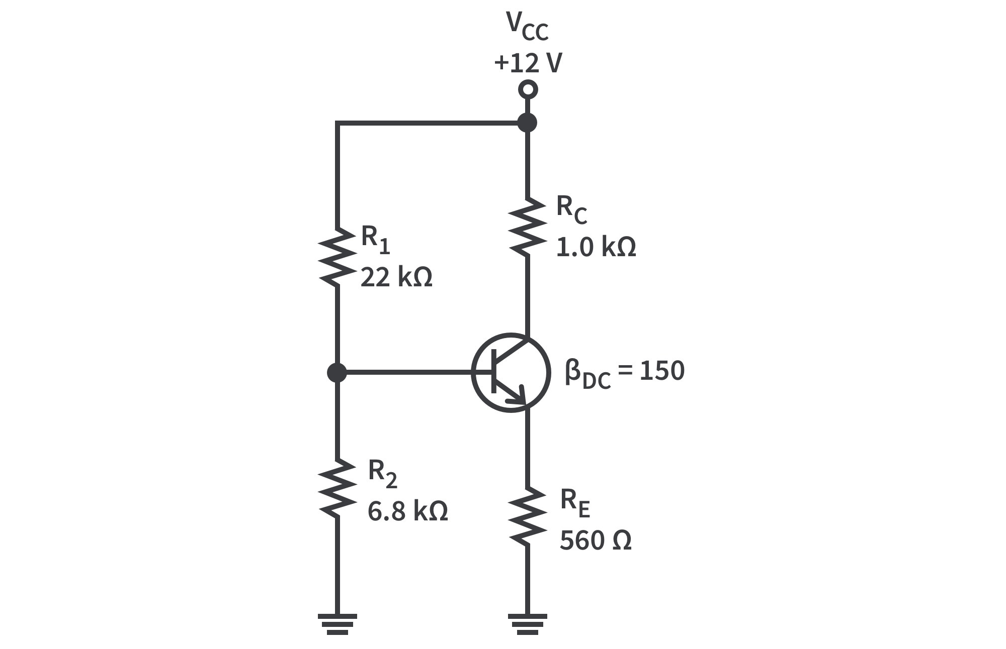
DC Analysis
The DC bias values must first be determined.
A DC equivalent circuit is developed by removing the capacitors because they appear open in DC bias. This also removes RL and the signal source. The DC equivalent circuit of Fig. 9 is shown in Fig. 10.
Figure 10: DC equivalent circuit for the amplifier in Fig. 9
Using Thevenin’s theorem, the bias circuit and applying Kirchhoff’s voltage law to the base-emitter circuit,
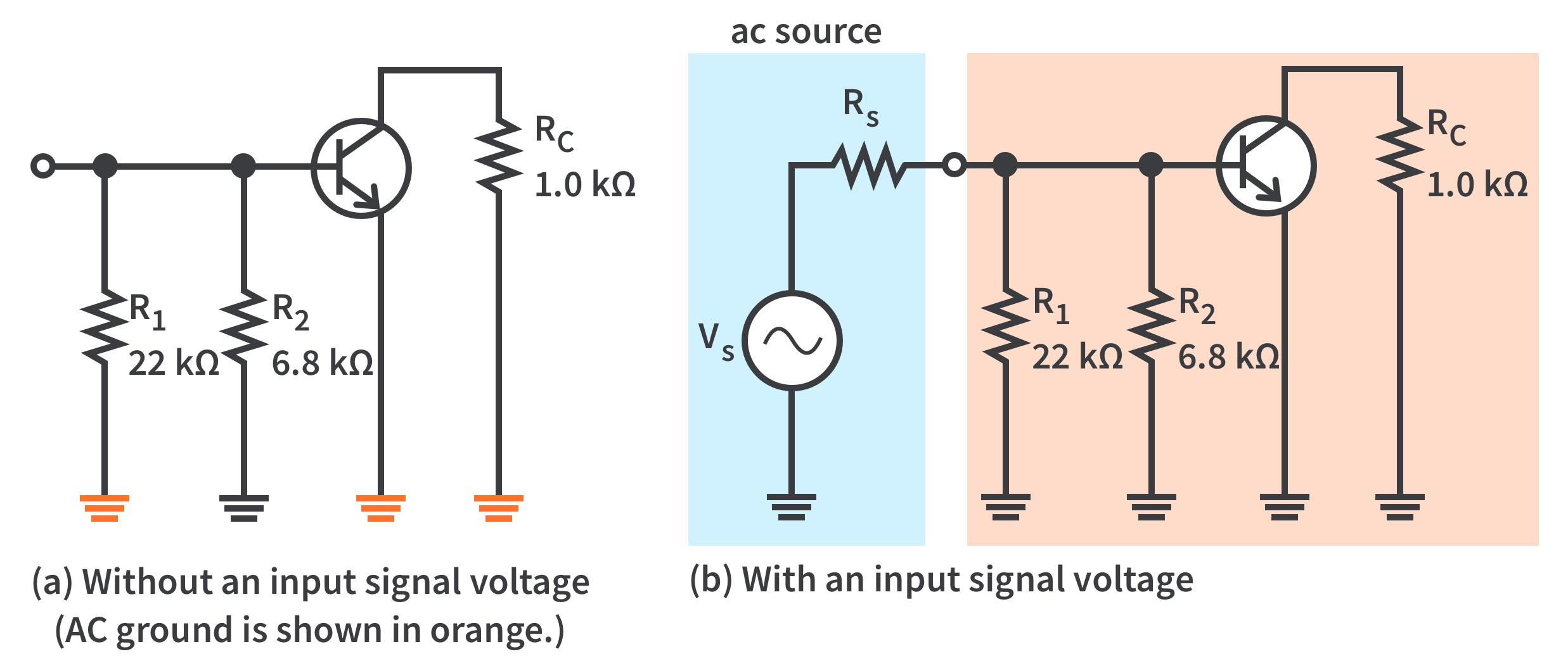
AC Analysis
An AC equivalent circuit is developed as follows:
The capacitors are replaced by effective shorts because their values are selected so that XC is negligible at the signal frequency.
The DC source is replaced by ground.
Figure 11: AC equivalent circuit for the amplifier in Figure 9
The AC ground and the actual ground are treated as the same point electrically.
The amplifier in Fig. 9 is called a common-emitter amplifier because C2 keeps the emitter at AC ground. Ground is the common point in the circuit.
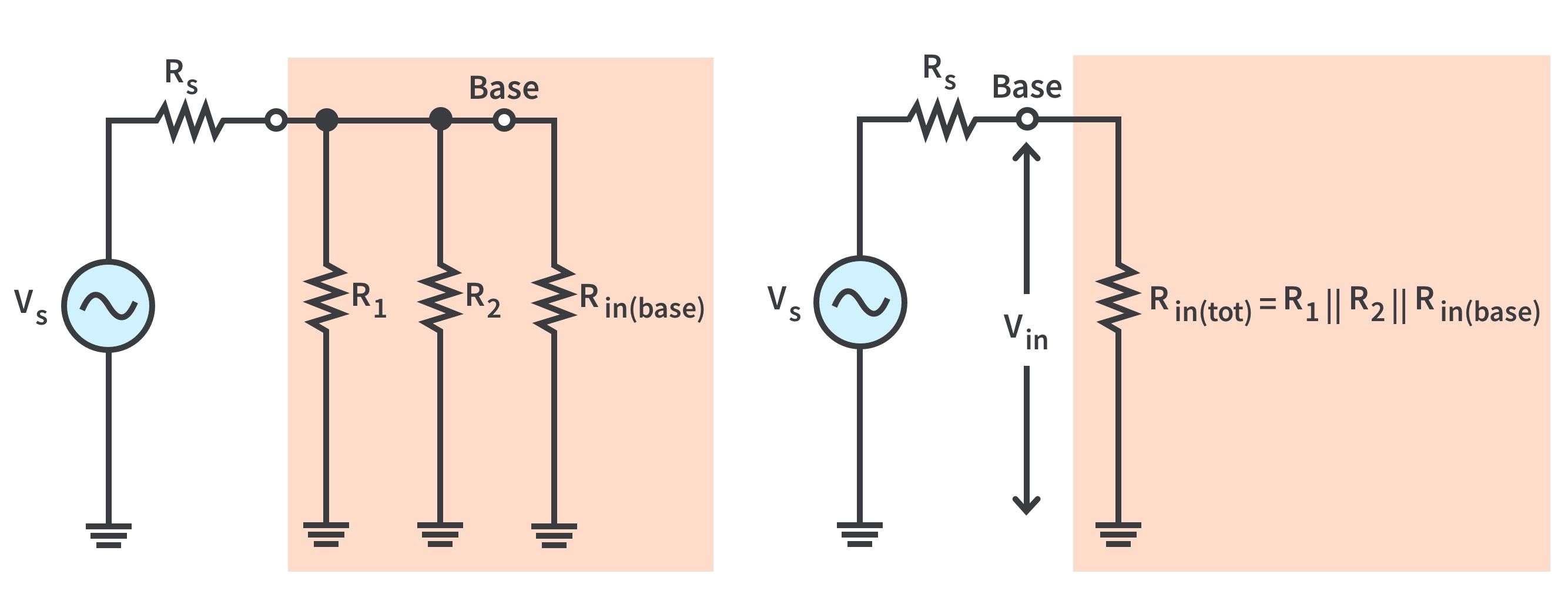
AC Voltage at the Base
If the internal resistance of the AC source is 0 then all of the source voltage appears at the base terminal.
If the AC source has a nonzero internal resistance, three factors must be taken into account in determining the actual signal voltage at the base:
the source resistance (Rs)
the bias resistance (R1||R2)
the AC input resistance at the base of the transistor (Rin(base))
This is illustrated in Fig. 12 and is simplified by combining R1, R2and Rin(base) in parallel to get the total input resistance, Rin(tot).
Figure 12: AC equivalent of the base circuit
The source voltage, Vs, is divided down by Rs and Rin(tot) so that the signal voltage at the base of the transistor is found by the voltage-divider formula
Input Resistance at the Base
Output Resistance
The output resistance of the common-emitter amplifier is the resistance looking in at the collector.
Actually, Rout=RC||r'c but since the internal AC collector resistance, r'c is typically much larger than RC, the approximation is usually valid.
Voltage Gain
The AC voltage gain expression for the common-emitter amplifier is developed using the model circuit in Fig. 13.
Figure 13: Model circuit for obtaining ac voltage gain
Voltage Gain Without the Bypass Capacitor
With the bypass capacitor, the gain of a given amplifier is maximum and equal to RC/r'e.
Without the bypass capacitor, the emitter is no longer at AC ground. RE is seen by the AC signal between the emitter and ground and adds to re' in the voltage gain formula.
The effect of RE is to decrease the AC voltage gain.
Effect of a Load on the Voltage Gain
When a resistor, RL, is connected to the output through the coupling capacitor C3 (Fig. 9), it creates a load on the circuit.
The collector resistance at the signal frequency is effectively RC in parallel with RL. The total AC collector resistance is
The voltage gain expression becomes
Stability of the Voltage Gain
Stability is a measure of how well an amplifier maintains its design values over changes in temperature or for a transistor with a different β.
There is a stability problem because the AC voltage gain is dependent on r'e which in turn depends on IE and temperature.
When r'e increases, the gain decreases and vice versa.
Swamping r'e to Stabilize the Voltage Gain
Swamping is used to minimize the effect of r'e without reducing the voltage gain to its minimum value.
This method “swamps” out the effect on the voltage gain; a compromise between having a bypass capacitor across RE and having no bypass capacitor at all.
The total external emitter resistance, RE, is formed with two emitter resistors, RE1 and RE2 . In Fig. 14, RE2 is bypassed and RE1 is not.
Figure 14: A swamped amplifier with a partially bypassed emitter resistance to minimize the effect of re' on the gain
If RE1 is at least ten times larger than re' then the effect of r'e is minimized and the approximate voltage gain for the swamped amplifier is
The Effect of Swamping on the Amplifier’s Input Resistance
The AC input resistance, looking in at the base of a common-emitter amplifier with RE completely bypassed is Rin = βacr'e.
When the emitter resistance is partially bypassed,
Current Gain
The current gain from base to collector is Ic/Ib or β. The overall current gain of the common-emitter amplifier is
Power Gain
The overall power gain is the product of the overall voltage gain (Av') and the overall current gain (Ai),
The Common-Collector Amplifier (Emitter-Follower)
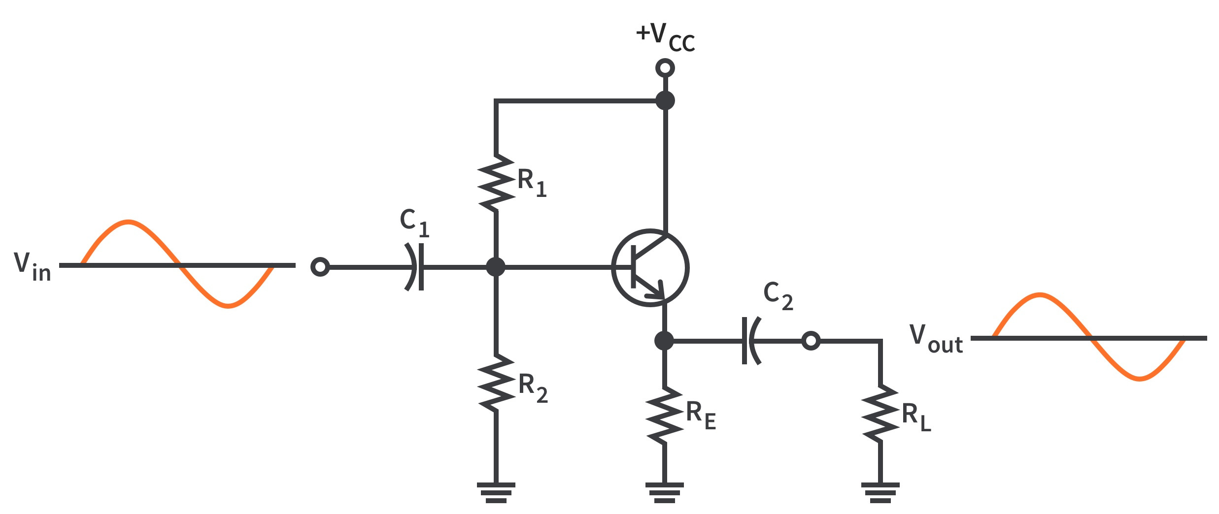
An emitter-follower circuit with voltage-divider bias is shown in Fig. 15.
The input signal is capacitively coupled to the base, the output signal is capacitively coupled from the emitter, and the collector is at ac ground.
There is no phase inversion, and the output is approximately the same amplitude as the input.
Figure 15: Emitter-follower with voltage-divider bias
Voltage Gain
The capacitive reactances are assumed to be negligible at the frequency of operation.
Since the output voltage is at the emitter, it is in phase with the base voltage, there is no inversion from input to output.
Because there is no inversion and because the voltage gain is approximately 1, the output voltage closely follows the input voltage in both phase and amplitude; thus the term emitter-follower.
Input Resistance
The emitter-follower is characterized by a high input resistance; this is what makes it a useful circuit.
If RE >> r'e , Rin(base) is equal to
It can be used as a buffer to minimize loading effects when a circuit is driving a low-resistance load.
The bias resistors in Fig. 15 appear in parallel with Rin(base), looking from the input source; and just as in the common-emitter circuit, the total input resistance is
Output Resistance
With the load removed, the output resistance, looking into the emitter of the emitter-follower, is approximated as:
The output resistance is very low, making the emitter-follower useful for driving low-resistance loads.
Current Gain
The current gain for the emitter-follower in Fig. 15 is
Power Gain
The common-collector power gain is the product of the voltage gain and the current gain.
For the emitter-follower, the power gain is approximately equal to the current gain because the voltage gain is approximately 1: Ap=AvAi.
Since Av ≈ 1, the power gain is
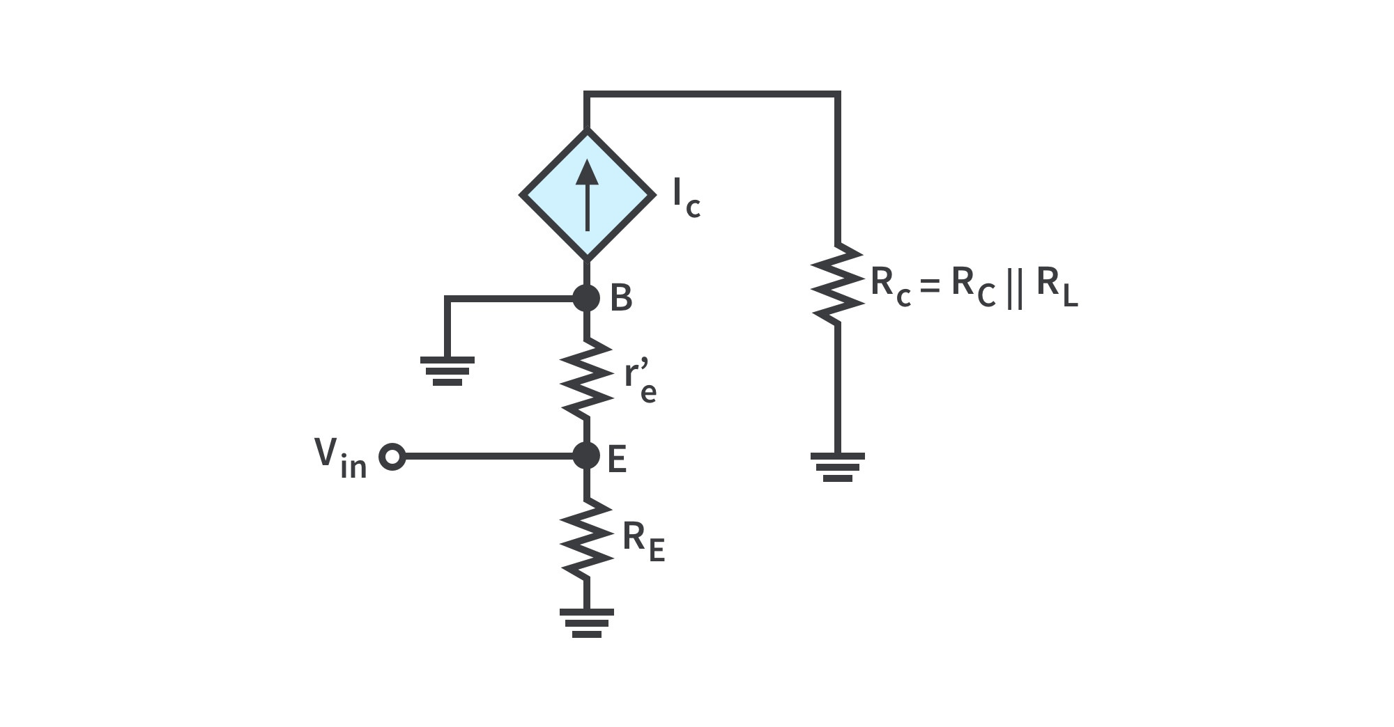
The Common-Base Amplifier
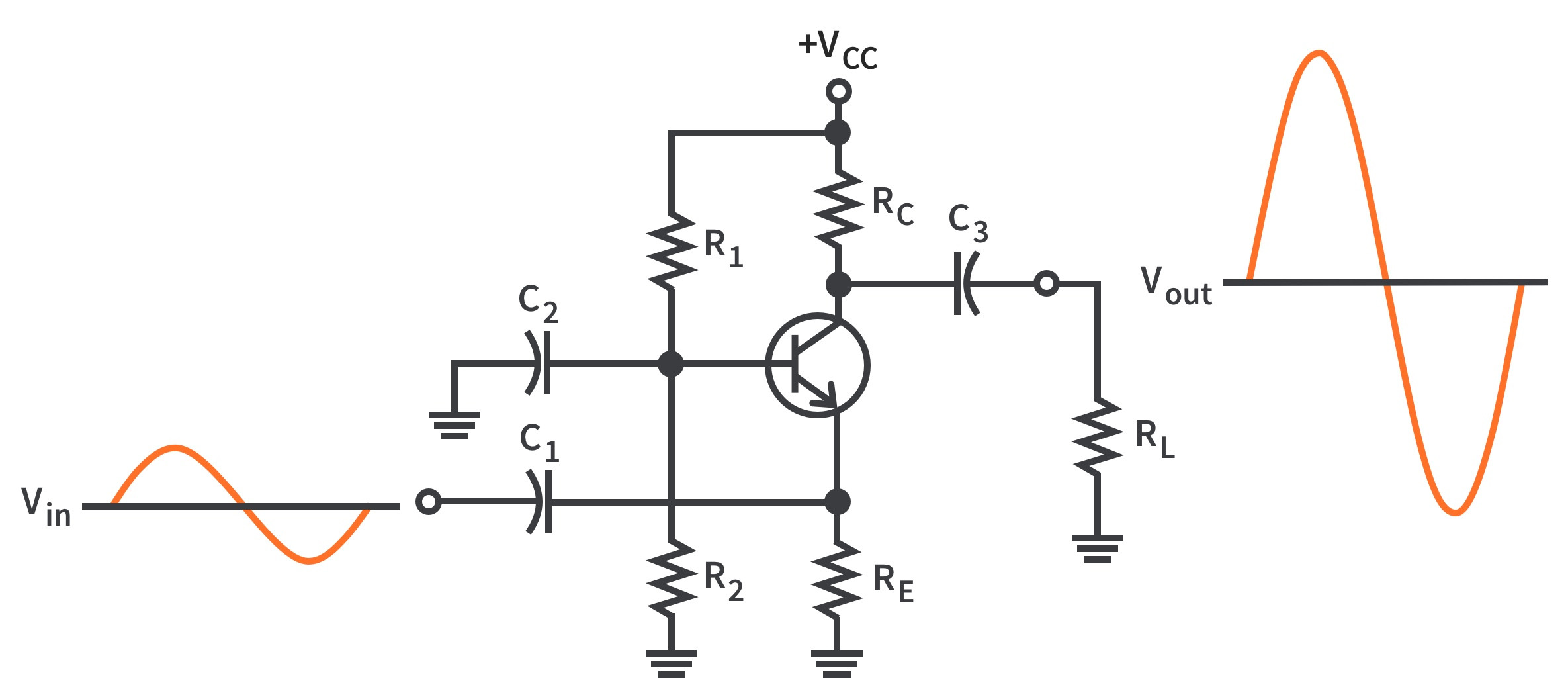
A typical common-base amplifier is shown in Fig. 16. The base is the common terminal and is at AC ground because of capacitor C2.
The input signal is capacitively coupled to the emitter. The output is capacitively coupled from the collector to a load resistor.
Figure 16(a): Common-base amplifier with voltage-divider biasFigure 16(b): AC equivalent model
Voltage Gain
The voltage gain from emitter to collector is developed as follows
If RE >>r'e, then
Input Resistance
The resistance, looking in at the emitter, is
If RE >> r'e, then
Output Resistance
Looking into the collector, the AC collector resistance, r'c, appears in parallel with RC. Typically, r'c is much larger than RC, so an approximation for the output resistance is
Current Gain
Ic is the AC output current, and Ie is the AC input current. Since Ic ≈ Ie , the current gain is approximately 1.
Power Gain
Since the current gain is approximately 1 for the common-base amplifier and Ap=AvAi , the power gain is approximately equal to the voltage gain.
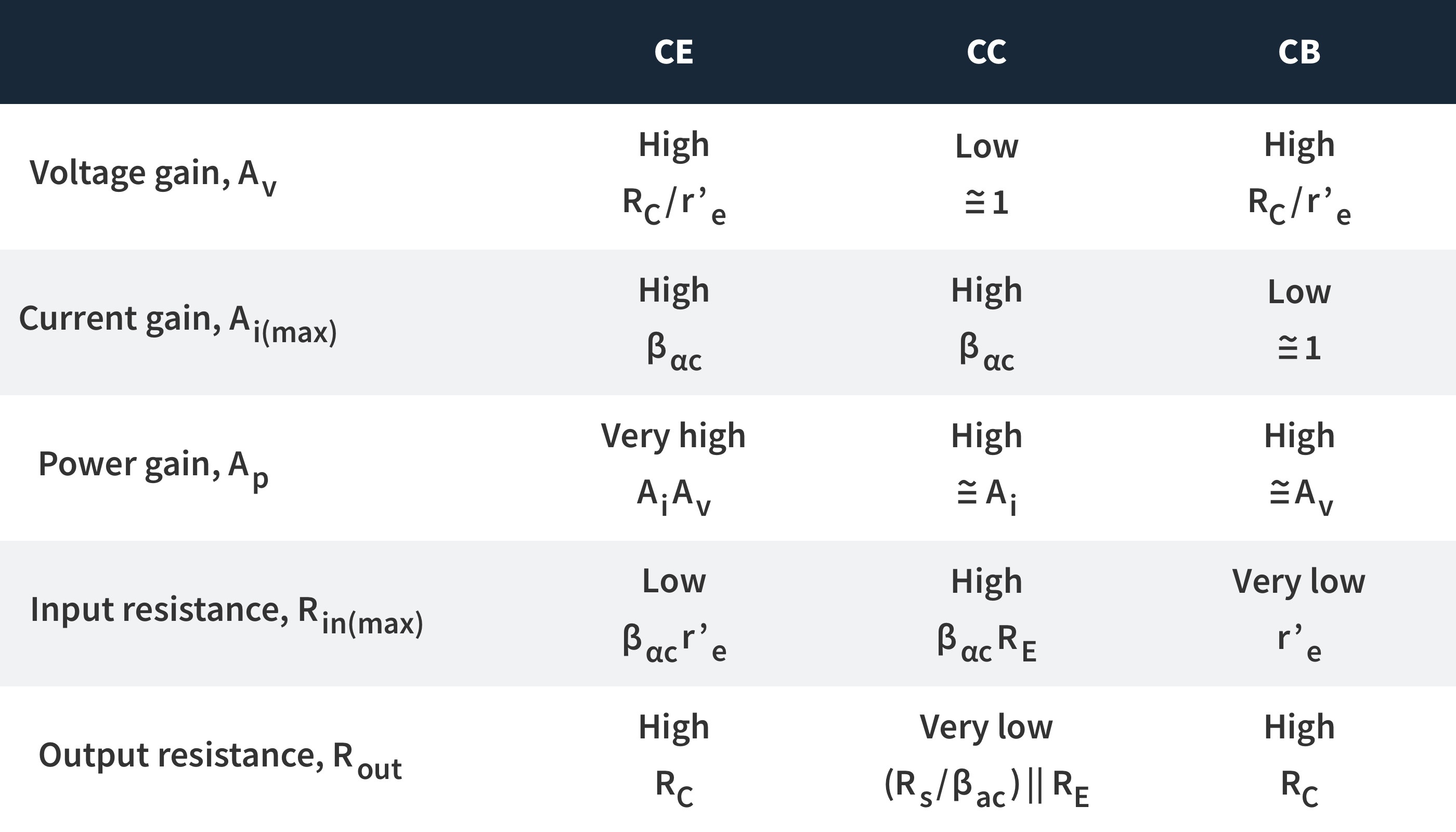
Summary of Amplifier Configurations
Figure 17: Summary of amplifier configurations
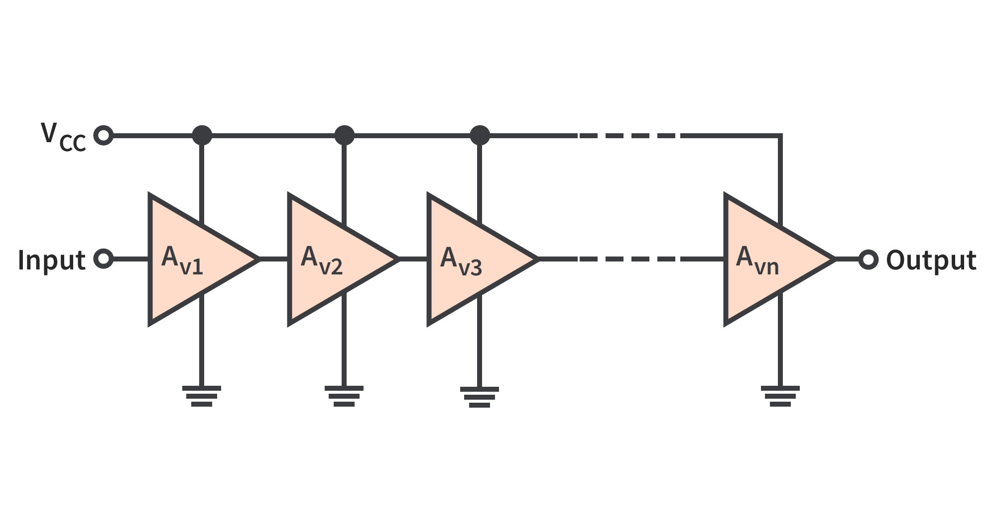
Multistage Amplifiers
Multistage Voltage Gain
The overall voltage gain, A'v, of cascaded amplifiers, as shown in Fig. 18, is the product of the individual voltage gains.
Figure 18: Cascaded amplifiers. Each triangular symbol represents a separate amplifier
Amplifier voltage gain is often expressed in decibels (dB) as follows:
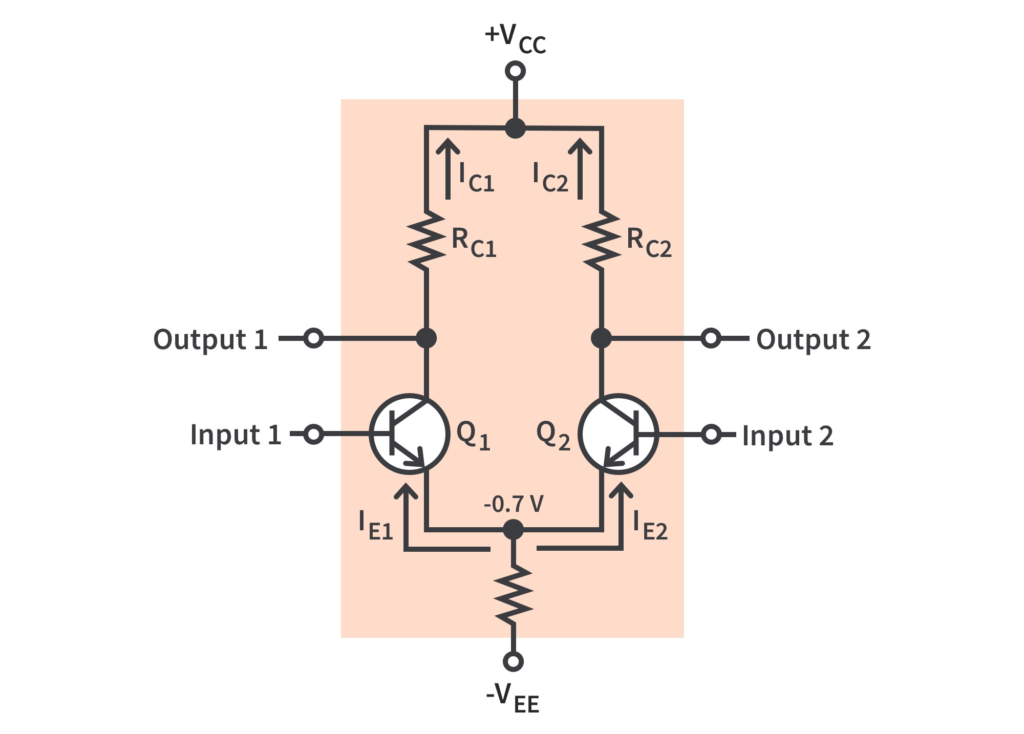
The Differential Amplifier
A differential amplifier produces outputs that are a function of the difference between two input voltages.
The differential amplifier has two basic modes of operation: differential (the two inputs are different) and common mode (the two inputs are the same).
Basic Operation
Figure 19: Basic differential amplifier with two inputs and two outputs
Output 1 = VC1 , Output 2 = VC2
When both inputs are grounded,
The DC emitter currents are the same when there is no input signal and
When input 2 is left grounded and a positive bias voltage is applied to input 1, the positive voltage on the base of Q1 increases IC1 and raises the emitter voltage to
This reduces the forward bias (VBE) of Q2, causing IC2 to decrease.
The net result is that the increase in IC1 causes a decrease in VC1, and the decrease in IC2 causes an increase in VC2.
When input 1 is grounded and a positive bias voltage is applied to input 2, the positive bias voltage causes Q2 to conduct more, increasing IC2.
The emitter voltage is also raised which reduces the forward bias of Q1 and causes IC1 to decrease.
The result is that the increase in IC2 produces a decrease in VC2, and the decrease in IC1 causes VC1 to increase.
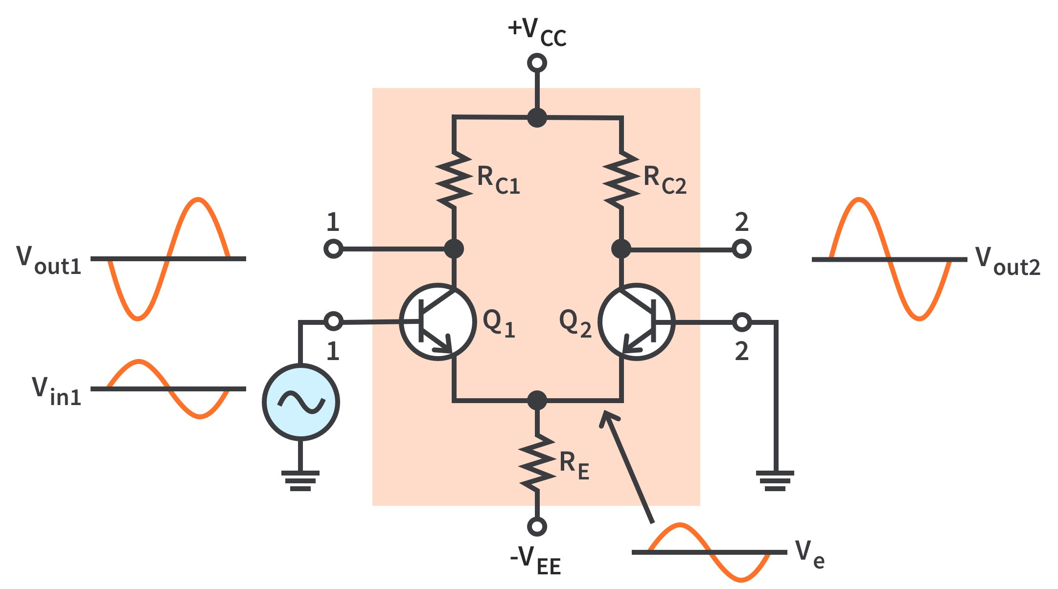
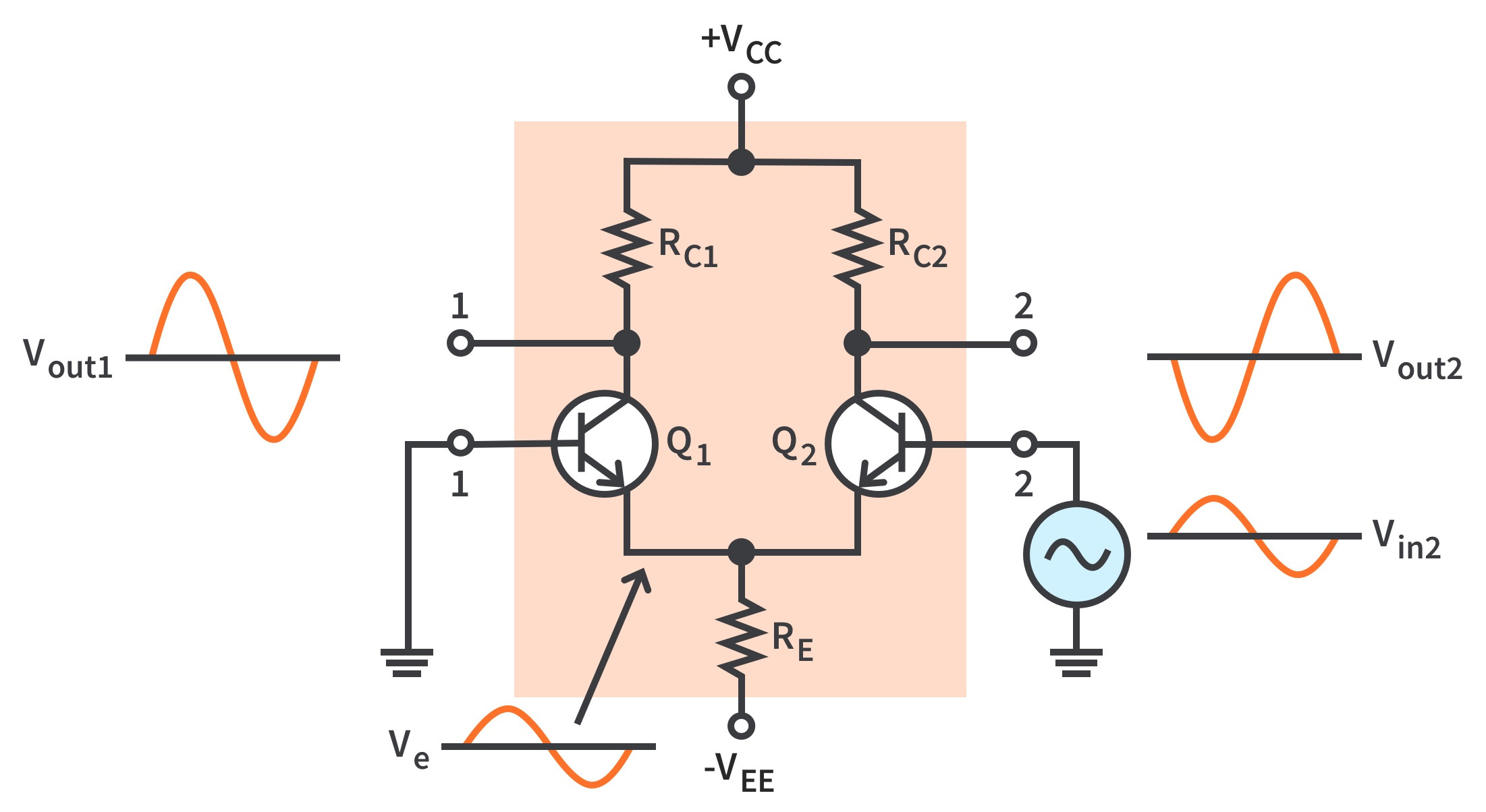
Single-Ended Differential Input
One input is grounded and the signal voltage is applied only to the other input.
In Fig. 20(a), an inverted, amplified signal voltage appears at output 1. Also, a signal voltage appears in phase at the emitter of Q1.
Since the emitters of Q1 and Q2 are common, the emitter signal becomes an input to Q2, which functions as a common-base amplifier. The signal is amplified by Q2 and appears non-inverted at output 2.
In Fig. 20(b), the signal is applied to input 2 with input 1 grounded. An inverted, amplified signal voltage appears at output 2.
Q1 acts as a common-base amplifier, and a non-inverted, amplified signal appears at output 1.
Figure 20(a): Single-ended differential input operation; the signal voltage is applied to input 1Figure 20(b): Single-ended differential input operation; the signal voltage is applied to input 2
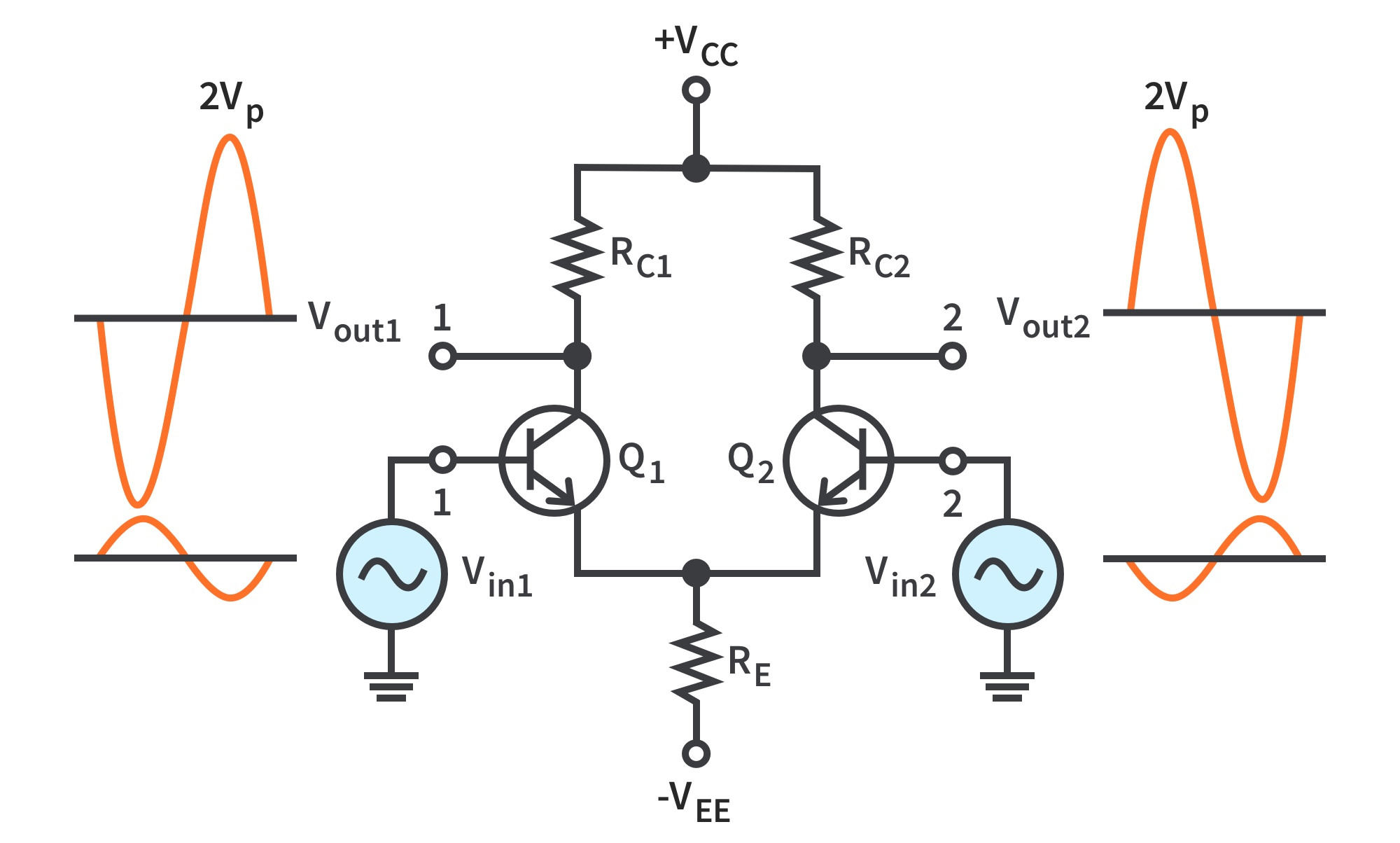
Double-Ended Differential Inputs
Two opposite-polarity (out-of-phase) signals are applied to the inputs.
The signal on either input acts alone as a single-ended input, producing output signals.
The output signals are obtained from superimposing both output 1 signals and both output 2 signals.
Figure 21: Double-ended differential operation
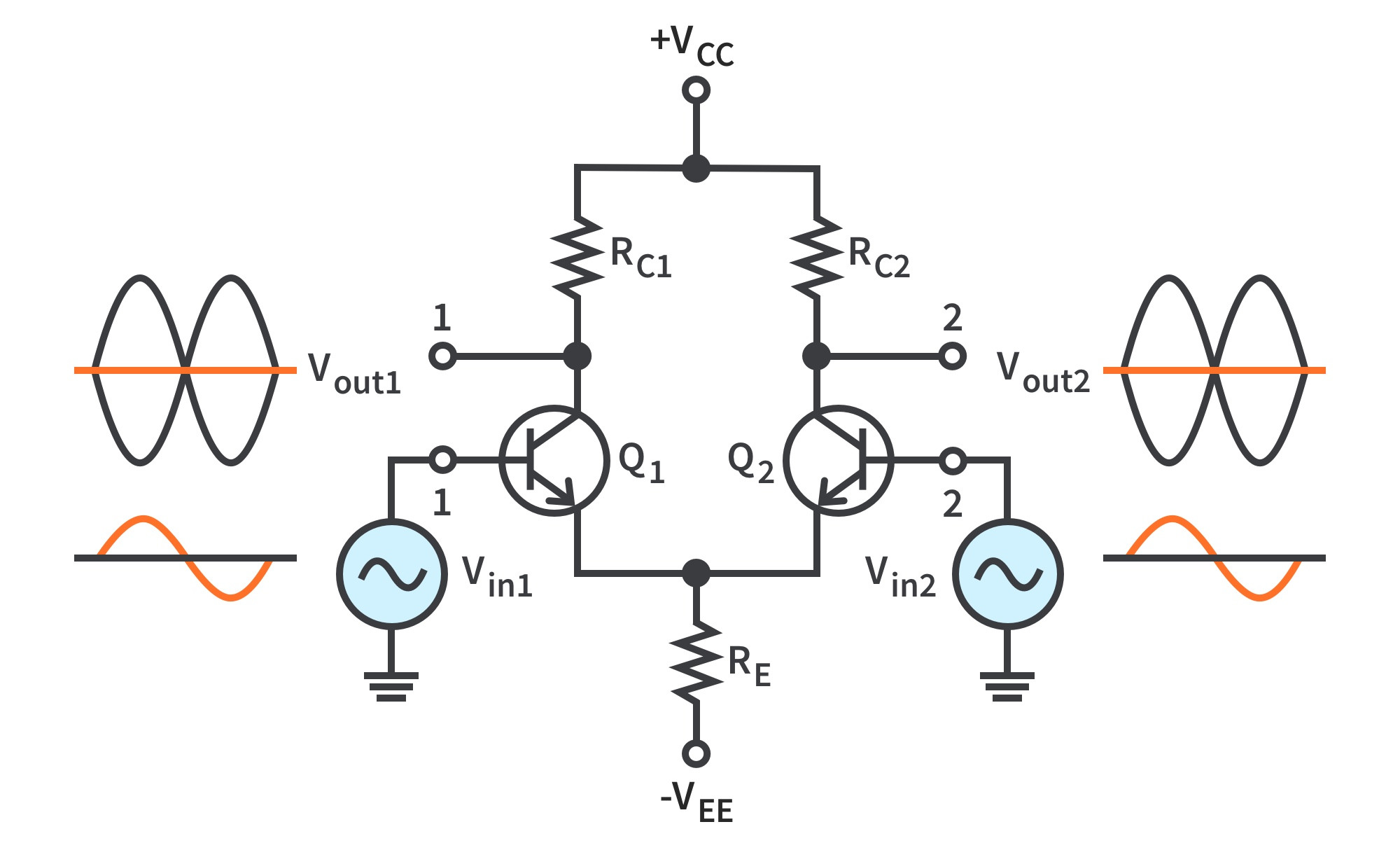
Common-Mode Inputs
The common-mode condition is when two signal voltages of the same phase, frequency, and amplitude are applied to the two inputs.
Considering each input signal as acting alone, the corresponding signals on output 1 are of the opposite polarity, and so are the ones on output 2.
Figure 22: Common-mode operation of a differential amplifier
When the input signals are applied to both inputs, the outputs are superimposed and they cancel, resulting in a zero output voltage.
Common-Mode Rejection Ratio
The measure of an amplifier’s ability to reject common-mode signals is a parameter called the CMRR (common mode rejection ratio).
The higher the value of CMRR, the better. The CMRR is often expressed in decibels (dB) as
Get the latest tools and tutorials, fresh from the toaster.