A diode is a two-terminal semiconductor device formed by two doped regions of silicon divided by a pn junction.
The p region is called the anode and is connected to a conductive terminal. The n region is called the cathode and is connected to a second conductive terminal.
Figure 1: Basic diode structure and schematic symbol
Diode Operation
Forward Bias
Forward bias is the condition that allows current through the pn junction.
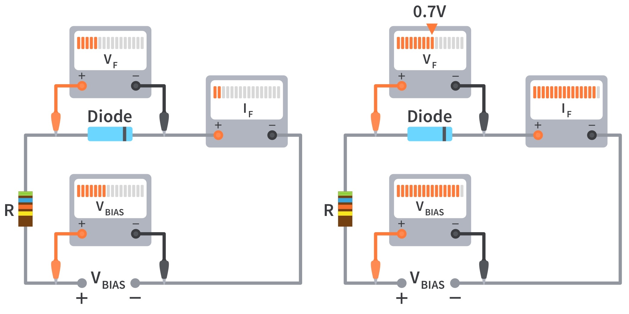
Fig. 2 shows a DC voltage source connected by conductive material (contacts and wire) across a diode in the direction to produce forward bias. The external bias voltage is designated as VBIAS. The resistor limits the forward current to a value that will not damage the diode.
Figure 2: A diode connected for forward bias
Requirements for forward bias:
The negative side of VBIAS is connected to the n region of the diode and the positive side is connected to the p region.
VBIAS must be greater than the barrier potential.
The depletion region narrows due to the reduction in negative and positive ions as majority carriers move toward the pn junction.
A voltage drop equal to the barrier potential (0.7 V for Silicon diode; 0.3 V for Germanium diode) is produced across the pn junction as electrons give up an amount of energy equivalent to the barrier potential when they cross the depletion region.
Diode Operation
Reverse Bias
Reverse bias is the condition that prevents current through the diode.
Fig. 3 shows a DC voltage source connected across a diode in the direction to produce reverse bias. This external bias voltage is designated as VBIAS just as it was for forward bias.
Figure 3: A diode connected for reverse bias
The positive side of VBIAS is connected to the n region of the diode and the negative side is connected to the p region. Note that the depletion region is shown much wider than in forward bias or equilibrium.
Voltage-Current Characteristic of a Diode
V-I Characteristic for Forward Bias
When a forward-bias voltage is applied across a diode, there is forward current; designated by IF. Fig. 4 illustrates what happens as the forward-bias voltage is increased positively from 0 V.
Figure 4: Forward-bias measurements show general changes in forward voltage and forward current as bias voltage is increased
With 0 V across the diode, IF =0.
As VBIAS increases, IF and the voltage across the diode (VF) increases. A portion of VBIAS is dropped across the limiting resistor.
When VBIAS is increased to a value where VF reaches approximately 0.7 V (barrier potential), IF begins to increase rapidly.
As VBIAS continues to increase, IF also increases very rapidly, but VF increases only gradually above 0.7 V. This small increase in VF is due to the voltage drop across the internal resistance of the semiconductive material.
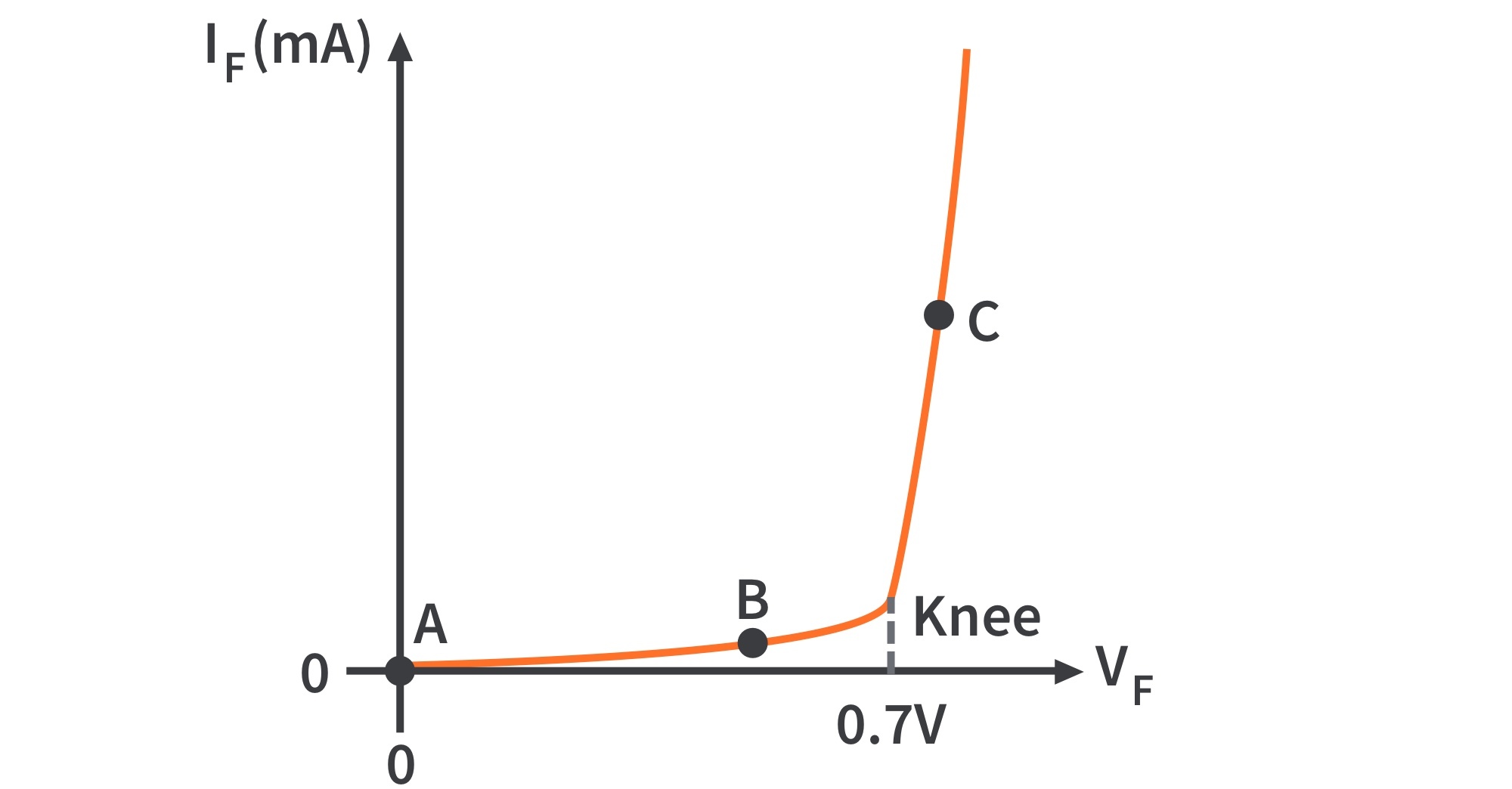
Graphing the V-I Curve
In Fig. 5, VF increases to the right along the horizontal axis, and IF increases upward along the vertical axis.
Figure 5: Relationship of voltage and current in a forward-biased diode.
IF increases very little until the forward voltage across the pn junction reaches approximately 0.7 V at the knee of the curve.
After this point, the forward voltage remains nearly constant at approximately 0.7 V, but IF increases rapidly. As previously mentioned, there is a slight increase in VF above 0.7 V.
Point A corresponds to a zero-bias condition. Point B is when VF is less than the barrier potential of 0.7 V. Point C is when VF is approximately equal to the barrier potential.
As VBIAS and IF continue to increase above the knee, VF will increase slightly above 0.7 V. In reality, VF can be as much as approximately 1 V, depending on the forward current.
Voltage-Current Characteristic of a Diode
V-I Characteristic for Reverse Bias
When a reverse-bias voltage is applied across a diode, there is only an extremely small reverse current (IR) through the pn junction.
With 0 V across the diode, IR=0.
As you gradually increase the reverse-bias voltage, there is a very small IR and the voltage across the diode increases.
When the applied bias voltage increases to a value where the reverse voltage across the diode (VR) reaches the breakdown value (VBR), IR begins to increase rapidly.
As the bias voltage continues to increase, IR also increases very rapidly, but the diode voltage increases very little above VBR.
Graphing the V-I Curve
VR increases to the left along the horizontal axis, and IR increases downward along the vertical axis.
Figure 6: V-I characteristic curve for a reverse-biased diode
There is very little IR (usually ) until VR reaches approximately VBR at the knee of the curve.
After this point, VR remains at approximately VBR, but IR increases very rapidly, resulting in overheating and possible damage if the current is not limited to a safe level.
VBR depends on the doping level, which the manufacturer sets, depending on the type of diode. A typical rectifier diode has a breakdown voltage of greater than 50 V. Some specialized diodes have a breakdown voltage that is only 5 V.
Voltage-Current Characteristic of a Diode
The Complete V-I Characteristic Curve
Combine the curves for both forward bias and reverse bias, and you have the complete V-I characteristic curve for a diode.
Figure 7: The complete V-I characteristic curve for a diode.
Temperature Effects
For a forward-biased diode, as the temperature is increased, IF increases for a given value of VF. Conversely, for a given value of IF, VF decreases.
For a reverse-biased diode, as temperature increases, IR increases.
Diode Models
The Ideal Diode Model
The least accurate approximation; can be represented by a simple switch
Forward-biased: diode acts like a closed (ON) switch; reverse-biased: diode acts like an open (OFF) switch, as shown in Fig. 8.
Figure 8: The ideal model of a diode
Although the barrier potential, the forward dynamic resistance, and the reverse current are all neglected, this model is adequate for most troubleshooting to determine if the diode is working properly.
The diode is assumed to have a zero voltage across it when forward-biased: VF=0 V. The forward current is determined by the bias voltage and the limiting resistor using Ohm’s law.
Since the reverse current is neglected, its value is assumed to be zero: IR = 0 A.
The reverse voltage equals the bias voltage: VR = VBIAS.
Diode Models
The Practical Diode Model or Constant Voltage Drop Model
includes the barrier potential
Forward-biased: diode is equivalent to a closed switch in series with a small equivalent voltage source (VF) equal to the barrier potential (0.7 V) with the positive side toward the anode.
When conducting, a voltage drop of 0.7 V appears across the diode.
Figure 9: The practical model of a diode
Reverse-biased: diode is equivalent to an open switch just as in the ideal model. The barrier potential does not affect reverse bias.
Since the barrier potential is included and the dynamic resistance is neglected, the diode is assumed to have a voltage across it when forward-biased: VF = 0.7 V.
The forward current is determined by first applying Kirchhoff’s voltage law to Figure 9(a):
The diode is assumed to have zero reverse current: IR = 0 A, VR = VBIAS.
The practical model is useful when troubleshooting in lower-voltage circuits. In these cases, the 0.7 V drop across the diode may be significant and should be taken into account.
Diode Models
The Complete Diode Model
the most accurate approximation; includes the barrier potential, small forward dynamic resistance (r'd) and large internal reverse resistance (r'R)
Forward-biased: diode acts as a closed switch in series with the equivalent barrier potential voltage (VB) and r'd.
Figure 10: The complete model of a diode
Reverse-biased: diode acts as an open switch in parallel with r'R. The barrier potential does not affect reverse bias.
The diode is assumed to have a voltage across it when forward-biased. This voltage (VF) consists of VB plus the small voltage drop across the dynamic resistance.
The voltage drop due to dynamic resistance increases as the current increases.
For the complete model of a silicon diode, the following formulas apply:
This model is generally suited to design problems using a computer for simulation.
Half-Wave Rectifiers
What is a half-wave rectifier?
A half-wave rectifier allows current through the load only during one-half of the cycle. It converts the AC input voltage (typically 120 V, 60 Hz) to a pulsating DC voltage, called a half-wave rectified voltage.
Half-Wave Rectifiers
Half-Wave Rectifier Operation
A diode is connected to an AC source and to a load resistor, RL, forming a half-wave rectifier.
When the sinusoidal input voltage (Vin) goes positive, the diode is forward-biased and conducts current through the load resistor.
Figure 11: During the positive alternation of Vin
The output voltage looks like the positive half of the input voltage. The current path is through the ground back to the source.
When the input voltage goes negative, the diode is reverse-biased. There is no current, so the voltage across the load resistor is 0 V.
Figure 12: During the negative alternation of Vin
The net result is that only the positive half-cycles of the AC input voltage appear across the load. Since the output does not change polarity, it is a pulsating DC voltage with a (standard) frequency of 60 Hz.
Half-Wave Rectifiers
Average Value of the Half-Wave Output Voltage
The average value of the half-wave rectified output voltage is the value measured on a DC voltmeter. Mathematically, it is the area under the curve over a full cycle, divided by the number of radians in a full cycle:
Effect of the Barrier Potential on the Half-Wave Rectifier Output
When the practical diode model is used with the barrier potential of 0.7 V, Vinmust overcome the barrier potential before the diode becomes forward-biased.
This results in a half-wave output with a peak value that is 0.7 V less than the peak value of the input. The expression for the peak output voltage is
Peak Inverse Voltage (PIV)
The PIV is the peak value of the input voltage, and the diode must be capable of withstanding this amount of repetitive reverse voltage.
The PIV occurs at the peak of each half-cycle of the input voltage when the diode is reverse-biased.
A diode should be rated at least 20% higher than the PIV.
Full-Wave Rectifiers
What is a full-wave rectifier?
A full-wave rectifier allows unidirectional (one-way) current through the load during the entire input cycle.
The result of full-wave rectification is an output voltage with a frequency twice the input frequency and that pulsates every half-cycle of the input.
Figure 13: Full-wave rectification
The number of positive alternations that make up the full-wave rectified voltage is twice that of the half-wave voltage for the same time interval. VAVG for a full-wave rectified sinusoidal voltage is twice that of the half-wave:
VAVG is approximately 63.7% of Vp for a full-wave rectified voltage.
Full-Wave Rectifiers
Center-Tapped Full-Wave Rectifier
A center-tapped rectifier is a type of full-wave rectifier that uses two diodes connected to the secondary of a center-tapped transformer.
Figure 14: A center-tapped full-wave rectifier
During positive half-cycles, D1 is forward-biased and D2 is reverse-biased. The current path is through D1 and the load resistor RL.
During negative half-cycles, D2 is forward-biased and D1 is reverse-biased. The current path is through D2 and RL.
Because the output current during both the positive and negative portions of the input cycle is in the same direction through the load, the output voltage developed across the load resistor is a full-wave rectified DC voltage.
The output voltage of a center-tapped full-wave rectifier is always one-half of the total secondary voltage less the diode drop.
Peak Inverse Voltage
Full-Wave Rectifiers
Bridge Full-Wave Rectifier
The bridge rectifier uses four diodes connected as shown in Fig. 15.
Figure 15: A bridge rectifier
When the input cycle is positive, D1 and D2 are forward-biased and conduct current. A voltage is developed across RL that looks like the positive half of the input cycle. During this time, diodes D3 and D4 are reverse-biased.
During the negative half-cycle of the input, D3 and D4 are forward-biased and conduct current. D1 and D2 are reverse-biased. A full-wave rectified output voltage appears across RLas a result of this action.
Bridge Output Voltage
Two diodes are always in series with the load resistor during both the positive and negative half-cycles. Taking diode drops into account, the output voltage is
Peak Inverse Voltage
Since the output voltage is ideally equal to the secondary voltage,
If the diode drops of the forward-biased diodes are included, the peak inverse voltage across each reverse-biased diode in terms of Vp(out) is
If the diode drop is neglected, the bridge rectifier requires diodes with half the PIV rating of those in a center-tapped rectifier for the same output voltage.
Diode Limiters and Clampers
Diode Limiters
Diode circuits, called limiters or clippers, are sometimes used to clip off portions of signal voltages above or below certain levels.
Fig. 16 shows a diode positive limiter that limits or clips the positive part of the input voltage.
Figure 16: Diode positive limiter
As the input voltage goes positive, the diode becomes forward-biased and conducts current. Point A is limited to +0.7 V when the input voltage exceeds this value.
When Vin goes back below 0.7 V, the diode is reverse-biased. Vout looks like the negative part of Vin, with a magnitude determined by the voltage divider formed by R1 and RL:
If the diode is turned around, the negative part of the input voltage is clipped off. When Vin goes above -0.7 V, the diode is no longer forward-biased; and a voltage appears across RL proportional to Vin.
Biased Limiters
The level to which an AC voltage is limited can be adjusted by adding a bias voltage, VBIAS, in series with the diode. The voltage at point A must equal VBIAS + 0.7 V before the diode will become forward-biased and conduct.
Once the diode begins to conduct, the voltage at point A is limited to VBIAS + 0.7 V so that all input voltage above this level is clipped off.
To limit a voltage to a specified negative level, the diode and bias voltage must be connected as shown below. In this case, the voltage at point A must go below -VBIAS - 0.7 V to forward-bias the diode and initiate limiting action.
Voltage-Divider Bias
The bias voltage sources that have been used to illustrate the basic operation of diode limiters can be replaced by a resistive voltage divider that derives the desired bias voltage from the DC supply voltage.
Figure 17: Diode limiters implemented with voltage-divider bias
The bias voltage is set by the resistor values according to the voltage-divider formula:
Diode Limiters and Clampers
Diode Clampers
A clamper adds a DC level to an AC voltage. Clampers are sometimes known as DC Restorers. Figure 18 shows a diode clamper that inserts a positive DC level in the output waveform.
Figure 18: Positive clamper operation
When the input voltage initially goes negative, the diode is forward-biased, allowing the capacitor to charge to near the peak of the input.
Just after the negative peak, the diode is reverse-biased because the cathode is held near Vp(in)-0.7 V by the charge on the capacitor.
The capacitor can only discharge through the high resistance of RL. So, from the peak of one negative half-cycle to the next, the capacitor discharges very little. The amount that is discharged depends on the value of RL.
If the diode is turned around, a negative DC voltage is added to the input voltage to produce the output voltage as shown in Figure 19.
Figure 19: Negative clamper
The net effect of the clamping action is that the capacitor retains a charge approximately equal to the peak value of the input less the diode drop.
The capacitor voltage acts essentially as a battery in series with the input voltage. The DC voltage of the capacitor adds to the input voltage by superposition.
Zener Diodes
A Zener diode is a silicon pn junction device that allows current to flow not only in the forward direction, but also in the reverse direction if the voltage is greater than the breakdown voltage known as the Zener knee voltage/Zener voltage.
Figure 20: Zener diode and schematic symbol
Zener Diode Operation
Zener diodes act like normal diodes when forward-biased.
Once the reverse voltage equals the Zener Voltage rating, Zener diodes are designed to allow current to flow in reverse.
Zener diodes are designed to operate in the breakdown region.
A Zener diode operating in breakdown acts as a voltage regulator because it maintains a nearly constant voltage, which is equal to the Zener voltage, across its terminals over a specified range of reverse-current values.
This constant voltage drop across the Zener diode produced by reverse breakdown is represented by a DC voltage symbol.
Get the latest tools and tutorials, fresh from the toaster.