An atom is the smallest particle of an element that retains the characteristics of that element. Each element has atoms that are different from the atoms of all other elements. This gives each element a unique atomic structure.
The Bohr Model
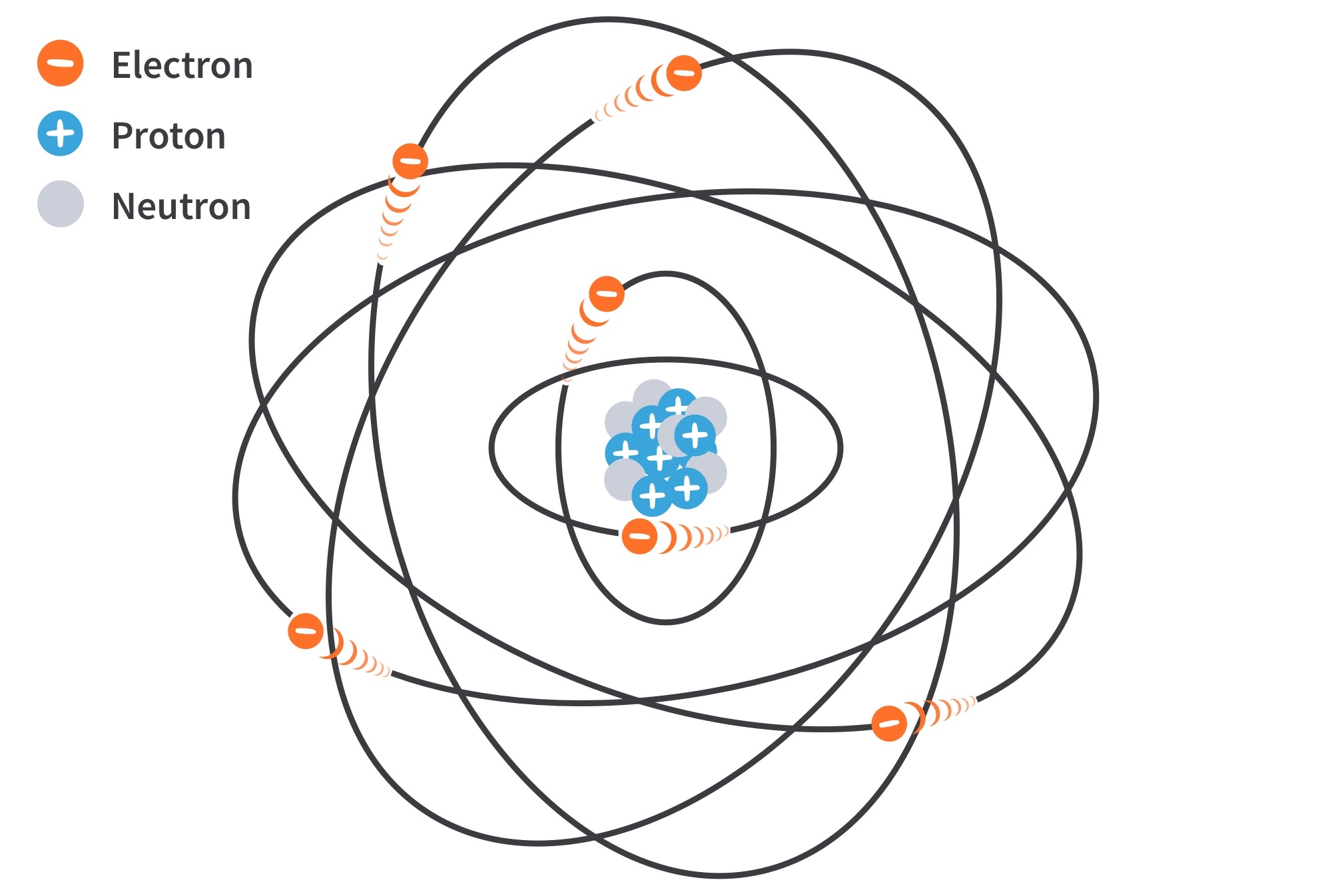
In the classical Bohr model, atoms have a planetary structure that consists of a central nucleus surrounded by orbiting electrons, as illustrated in Fig. 1.
Figure 1: The Bohr model of an atom. The “tails” on the electrons indicate motion.
The nucleus consists of positively charged particles called protons and uncharged particles called neutrons. The basic particles of negative charge that circle the nucleus are called electrons.
Atomic Number
The number of protons in the nucleus; the same as the number of electrons in an electrically balanced (neutral) atom.
All elements are arranged in the periodic table of the elements in order according to their atomic number.
In their neutral state, all atoms of an element have the same number of electrons as protons, for a net charge of zero.
Energy Levels
Only discrete values of electron energies exist within atomic structures thus electrons must only orbit at discrete distances from the nucleus.
Each discrete distance (orbit) from the nucleus corresponds to a certain energy level.
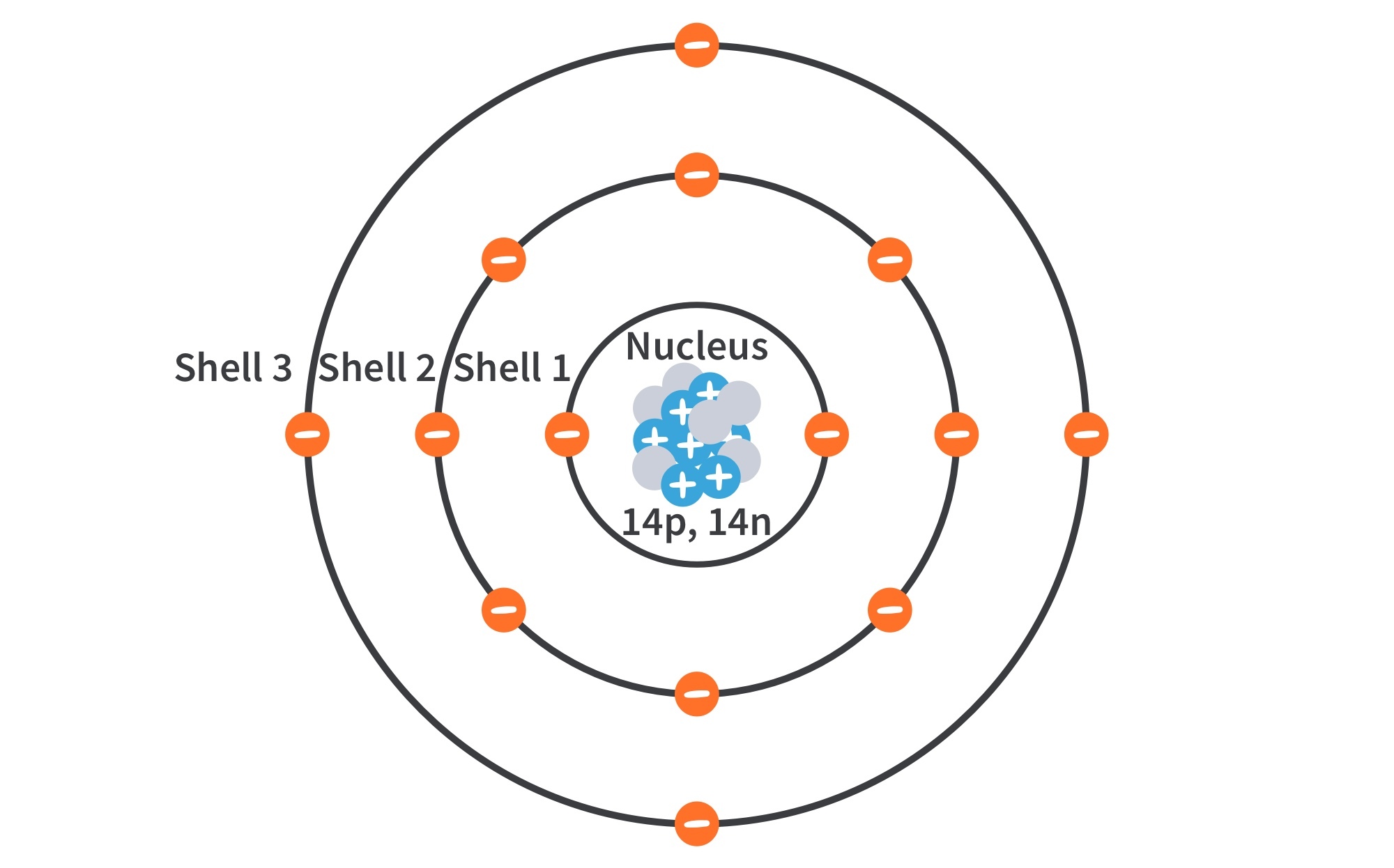
The orbits are grouped into energy levels known as shells. A given atom has a fixed number of shells; each shell has a fixed maximum number of electrons.
Figure 2: Illustration of the Bohr model of the silicon atom.
Shells are designated 1, 2, 3, and so on, with 1 being closest to the nucleus. Electrons near the nucleus have less energy than those in more distant orbits.
The Maximum Number of Electrons in Each Shell (Ne) can be calculated by the formula,
Valence Electrons
Attractive force between the positively charged nucleus and the negatively charged electron decreases with increasing distance from the nucleus.
Electrons with the highest energy exist in the outermost (valence ) shell of an atom and are relatively loosely bound to the atom. These are called valence electrons.
Valence electrons contribute to chemical reactions and bonding which determine electrical properties.
When a valence electron gains sufficient energy from an external source, it can break free from its atom. This is the basis for conduction in materials.
Ionization
When an atom absorbs energy, the energies of the electrons are raised. If a valence electron acquires a sufficient amount of energy, called ionization energy, it can actually escape from the atom’s influence.
The process of losing a valence electron is known as ionization, and the resulting positively charged atom is called a positive ion.
The escaped valence electron is called a free electron. The reverse can occur when a free electron collides with an atom and is captured, releasing energy. The atom that acquired the extra electron is called a negative ion.
Materials Used in Electronics
Insulators, Conductors, and Semiconductors
An insulator does not conduct electrical current under normal conditions. Most insulators are compounds and have very high resistivities. Valence electrons are tightly bound to the atoms and there are very few free electrons. Examples: rubber, plastics, glass, mica, quartz.
A conductor easily conducts electrical current. Most metals are good conductors. The best conductors are single-element materials, such as copper (Cu), silver (Ag), gold (Au), and aluminum (Al), characterized by atoms with one valence electron very loosely bound to the atom. These loosely bound valence electrons become free electrons.
A semiconductor in its pure (intrinsic) state is neither a good conductor nor a good insulator. Single-element semiconductors are (characterized by atoms with four valence electrons) antimony (Sb), arsenic (As), astatine (At), boron (B), polonium (Po), tellurium (Te), silicon (Si), and germanium (Ge). Compound semiconductors such as gallium arsenide, indium phosphide, gallium nitride, and silicon germanium are also commonly used. Silicon is the most commonly used semiconductor.
Materials Used in Electronics
Band Gap
The energy difference between the valence band and the conduction band is the energy gap or band gap; the amount of energy that a valence electron must acquire to jump from the valence band to the conduction band.
Once in the conduction band, the electron is free to move throughout the material.
The band gap contains energy levels “not allowed” by quantum theory. It is a region in insulators and semiconductors where no electron states exist, although an electron can “jump” across it under certain conditions.
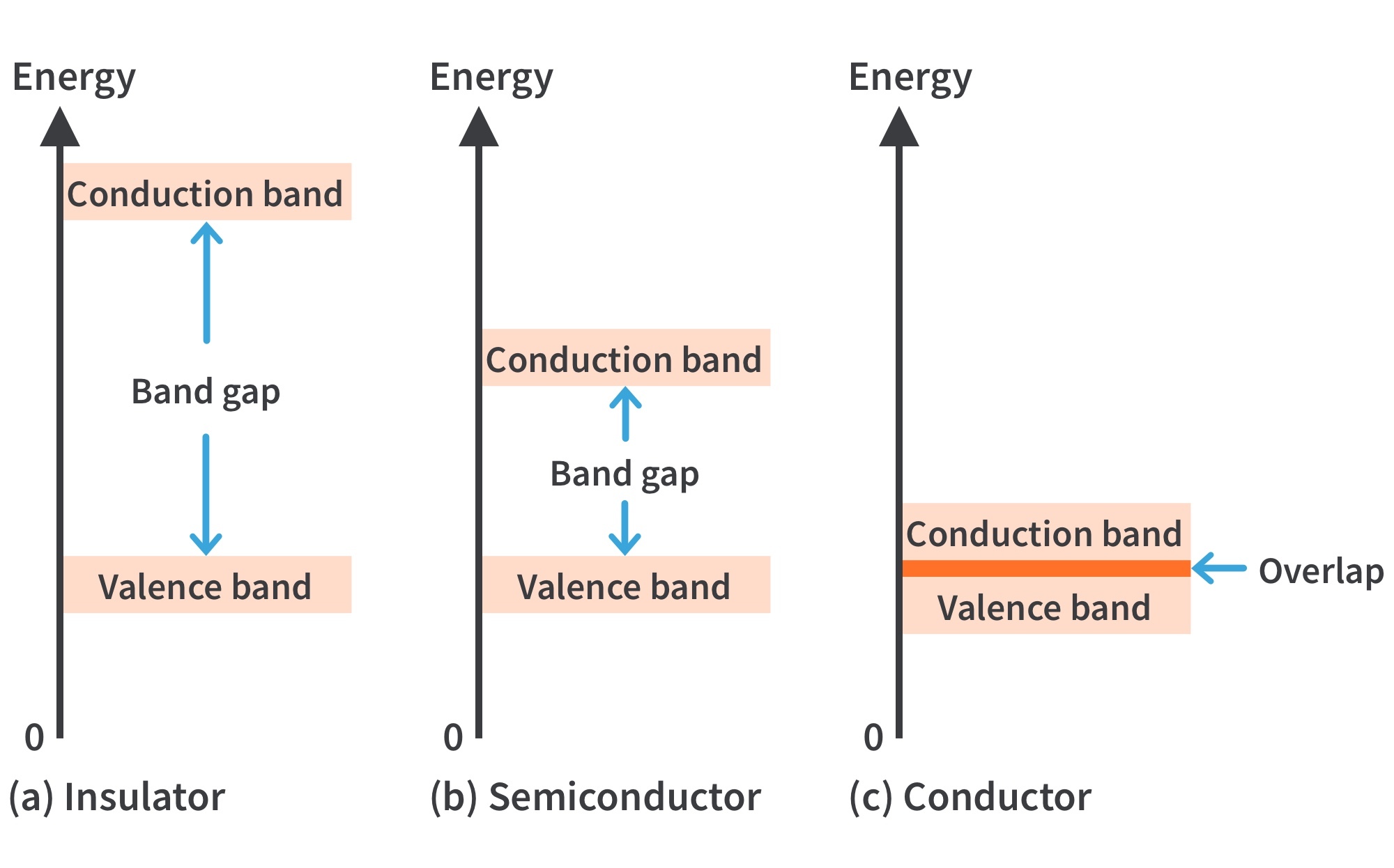
Figure 3: Energy diagrams for the three types of materials.
In semiconductors, the band gap is smaller, allowing an electron in the valence band to jump into the conduction band if it absorbs a photon. The band gap depends on the semiconductor material.
In conductors, the conduction band and valence band overlap, so there is no gap. Electrons in the valence band move freely into the conduction band, so there are always electrons available as free electrons.
Materials Used in Electronics
Semiconductor Atom and Conductor Atom
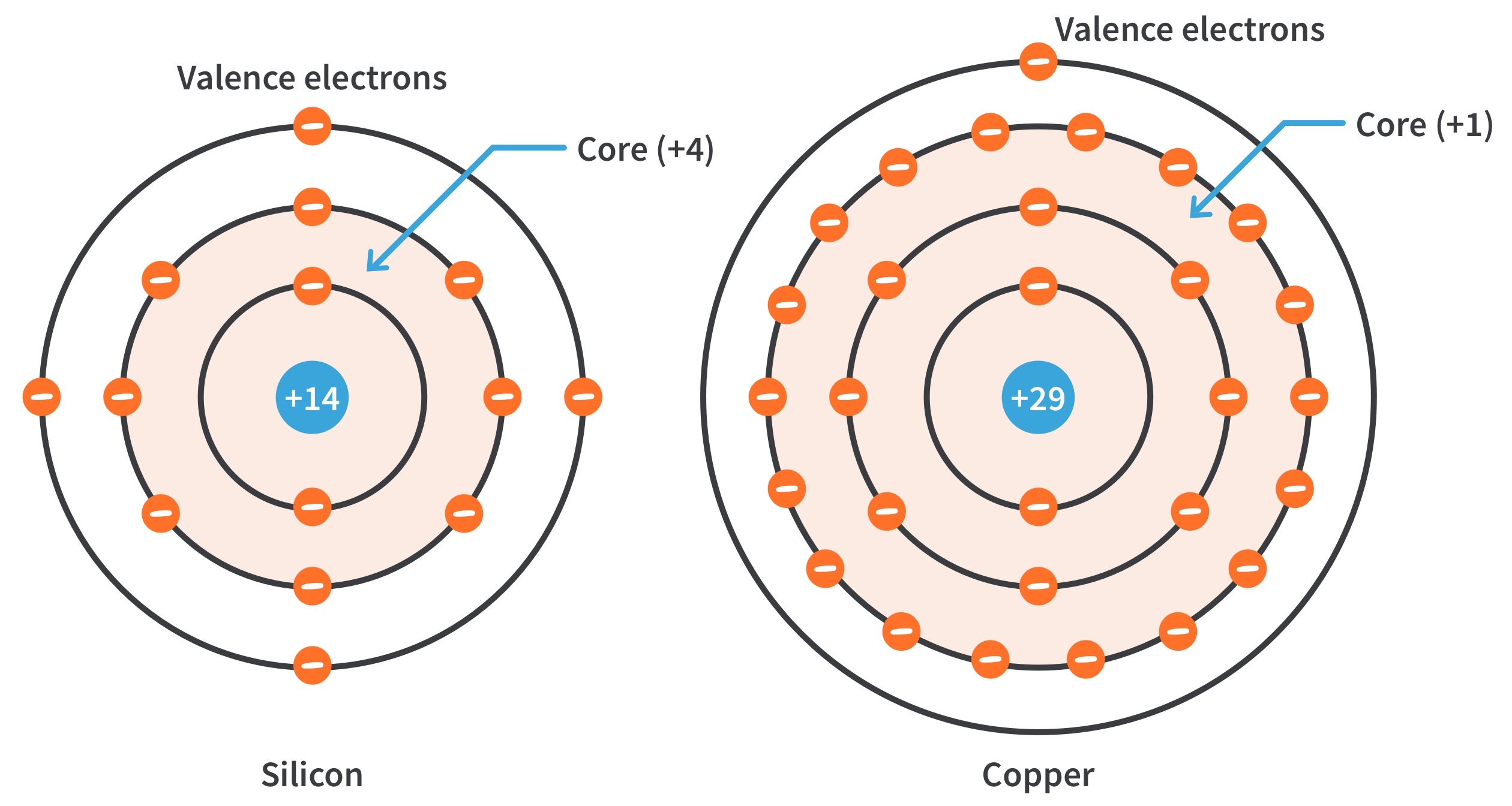
Silicon is a semiconductor and copper is a conductor. Bohr diagrams of the silicon atom and the copper atom are shown in Fig. 4.
Figure 4: Bohr diagrams of the silicon and copper atoms.
The core of the silicon atom has a net charge of 4 (14 p+, 10 e-) and the core of the copper atom has a net charge of 1 (29 p+, 28 e-). The core includes everything except the valence electrons.
There is more force trying to hold a valence electron to the atom in silicon than in copper.
The copper’s valence electron is in the 4th shell, while silicon’s valence electrons are in the 3rd shell. Thus the valence electron in copper has more energy than the valence electrons in silicon.
It is easier for valence electrons in copper to acquire enough additional energy to escape from their atoms and become free electrons.
Materials Used in Electronics
Silicon and Germanium
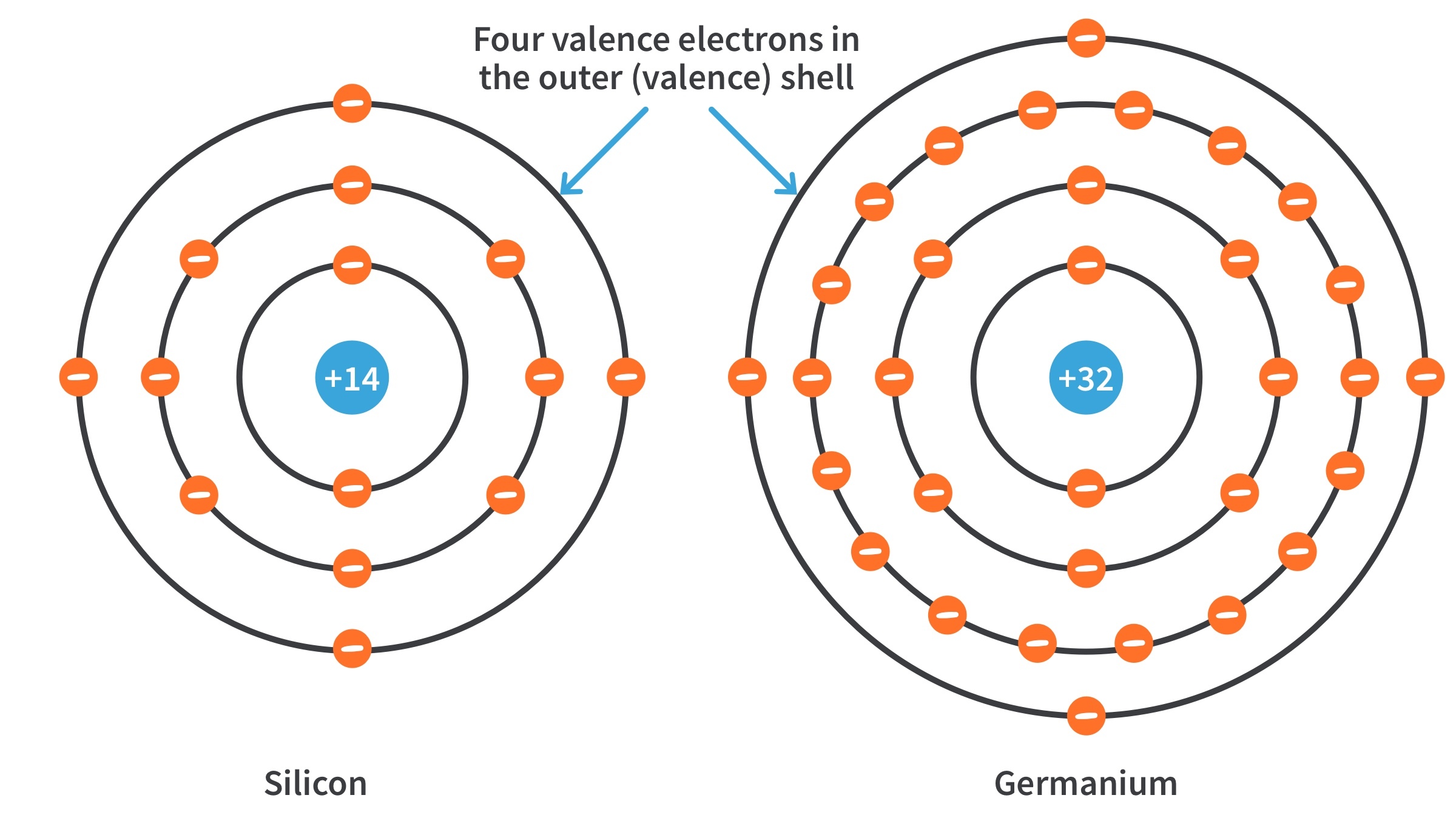
The atomic structures of silicon and germanium are compared in Fig. 5.
Figure 5: Diagrams of the silicon and germanium atoms.
Both silicon and germanium have the characteristic four valence electrons.
Germanium is more unstable at high temperatures as its valence electrons are at higher energy levels and require a smaller additional energy to escape from the atom. This is why silicon is the more widely used semiconductor.
Materials Used in Electronics
Covalent Bonds
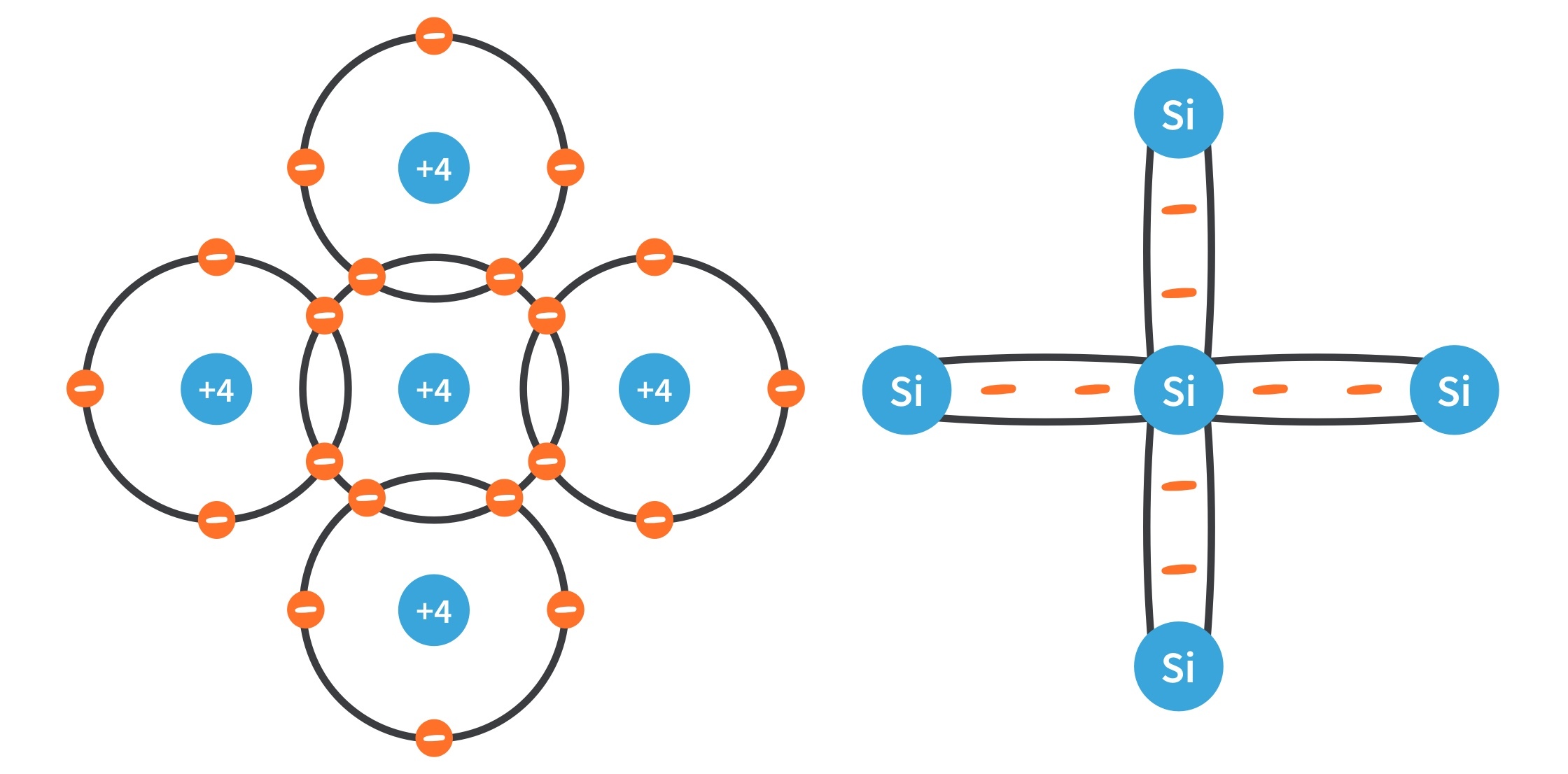
Sharing of valence electrons produces the covalent bonds that hold the atoms together; each valence electron is attracted equally by the two adjacent atoms which share it.
In Fig. 6, The center silicon atom shares an electron with four surrounding silicon atoms, creating a covalent bond with each. The surrounding atoms are in turn bonded to other atoms, and so on.
Figure 6: Silicon atom with four adjacent silicon atoms to form a crystal. The red negative signs represent the shared valence electrons.
Covalent bonding for germanium is similar because it also has four valence electrons.
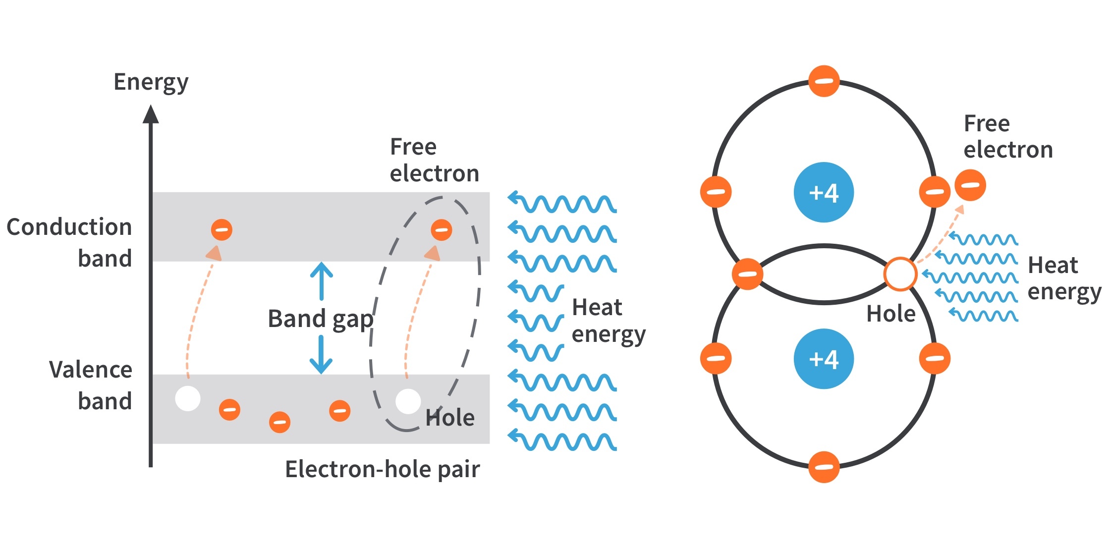
Current in Semiconductors
Conduction Electrons and Holes
An intrinsic (pure) silicon crystal at room temperature has sufficient heat energy for some valence electrons to jump the gap from the valence band into the conduction band, becoming free electrons.
Free electrons are also called conduction electrons. This is illustrated in the diagrams in Fig. 7.
Figure 7: Creation of electron-hole pairs in a silicon crystal. Electrons in the conduction band are free electrons.
When an electron jumps to the conduction band, a vacancy is left in the valence band within the crystal. This vacancy is called a hole.
For every electron raised to the conduction band by external energy, there is one hole left in the valence band, creating what is called an electron-hole pair.
Recombination occurs when a conduction-band electron loses energy and falls back into a hole in the valence band.
Intrinsic silicon at room temperature has free electrons that are unattached to any atom and are drifting randomly throughout the material.
There is an equal number of holes in the valence band created when these electrons jump into the conduction band.
Current in Semiconductors
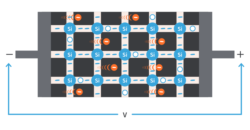
Electron and Hole Current
Electron current
When a voltage is applied across a semiconductor, the free electrons are easily attracted toward the positive end. This movement of free electrons in a semiconductive material is called electron current.
Figure 8: Electron current in intrinsic silicon is produced by the movement of thermally generated free electrons.
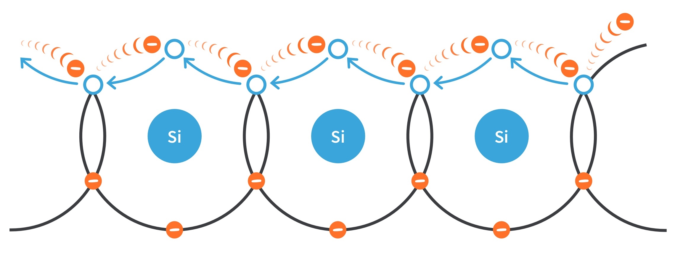
Hole Current
Electrons in the valence band are still attached to atoms and are not free to move randomly like the free electrons. However, a valence electron can move into a nearby hole with little change in its energy level, leaving another hole where it came from. Effectively, the hole has moved from one place to another in the crystal structure.
Figure 9: Hole current in intrinsic silicon
N-type and P-type Semiconductors
Conductivity of semiconductors can be increased by the controlled addition of impurities to the intrinsic semiconductive material. This process, called doping, increases the number of current carriers (electrons or holes).
N-Type Semiconductor
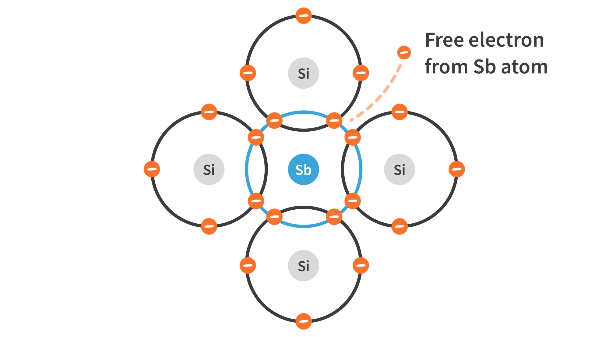
To increase the number of conduction-band electrons in intrinsic silicon, pentavalent impurities are added. These are atoms with five valence electrons such as arsenic (As), phosphorus (P), bismuth (Bi), and antimony (Sb).
As illustrated in Fig. 10, each pentavalent atom (antimony) forms covalent bonds with four adjacent silicon atoms, leaving one extra electron. This extra electron becomes a conduction electron.
Figure 10: Pentavalent impurity atom in a silicon crystal structure. An antimony (Sb) atom is shown in the center.
Because the pentavalent atom gives up an electron, it is often called a donor atom.
A conduction electron created by this doping process does not leave a hole in the valence band because it is in excess of the number required to fill the valence band.
The electrons are called the majority carriers in n-type material since most of the current carriers are electrons (the n stands for negative charge).
There are a few holes created when electron-hole pairs are thermally generated. Holes in an n-type material are called minority carriers.
P-Type Semiconductor
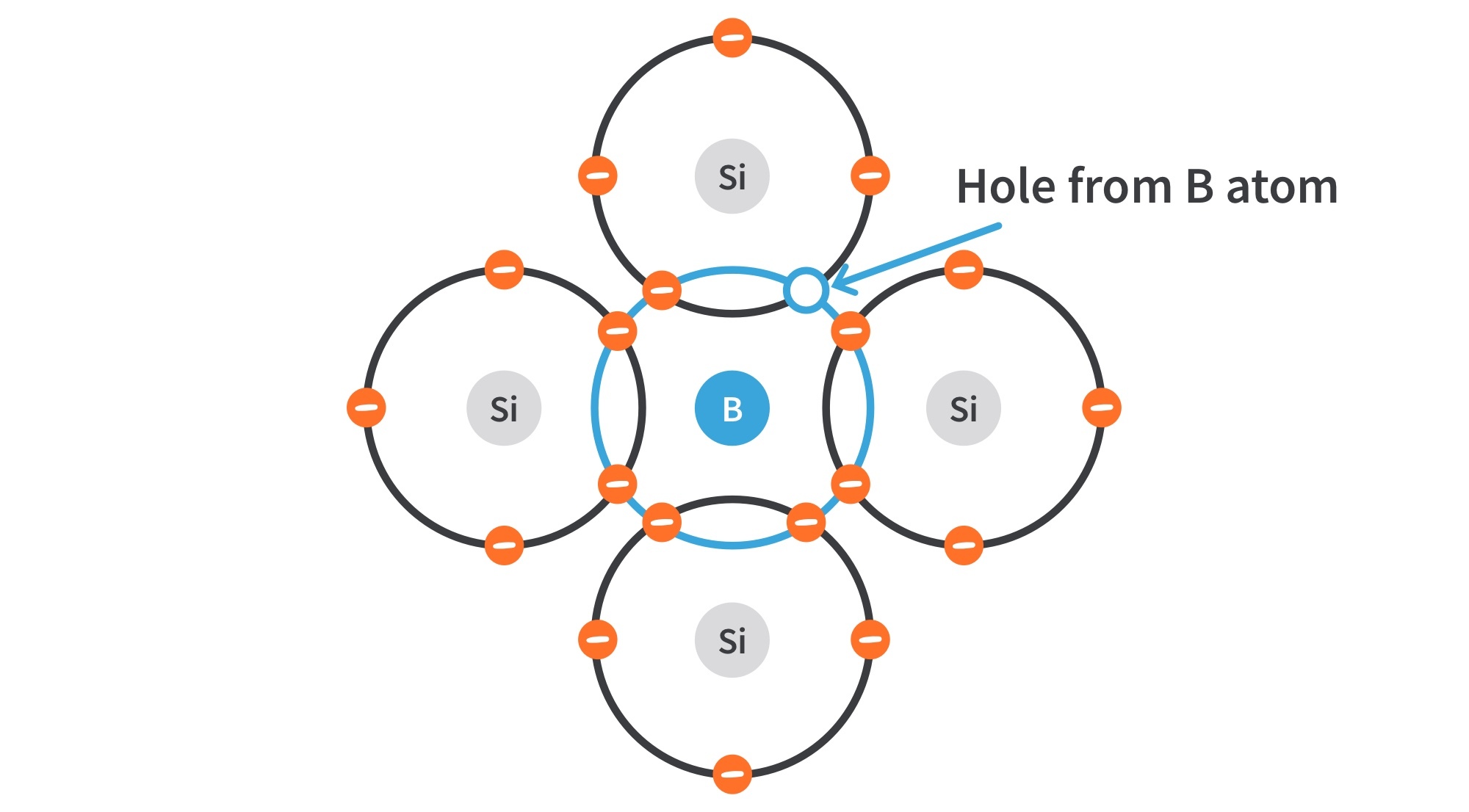
To increase the number of holes in intrinsic silicon, trivalent impurity atoms are added. These are atoms with three valence electrons such as boron (B), indium (In), and gallium (Ga).
As illustrated in Fig. 11, each trivalent atom (boron) forms covalent bonds with four adjacent silicon atoms. All three of the boron atom’s valence electrons are used in the bonds, and a hole results.
Figure 11: Trivalent impurity atom in a silicon crystal structure. A boron (B) impurity atom is shown in the center.
Because the trivalent atom can take an electron, it is often referred to as an acceptor atom.
A hole created by this doping process is not accompanied by a conduction (free) electron.
The holes are the majority carriers in p-type material since most of the current carriers are holes.
There are a few conduction-band electrons created when electron-hole pairs are thermally generated. Conduction-band electrons in p-type material are the minority carriers.
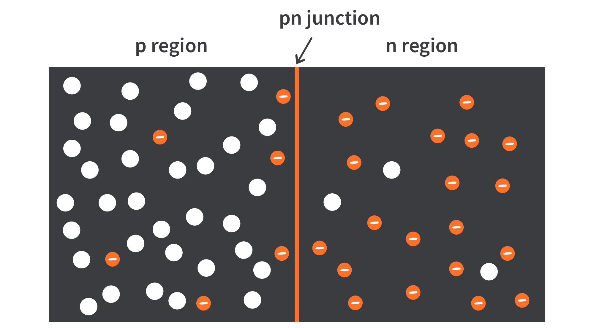
The PN Junction
What is a PN Junction?
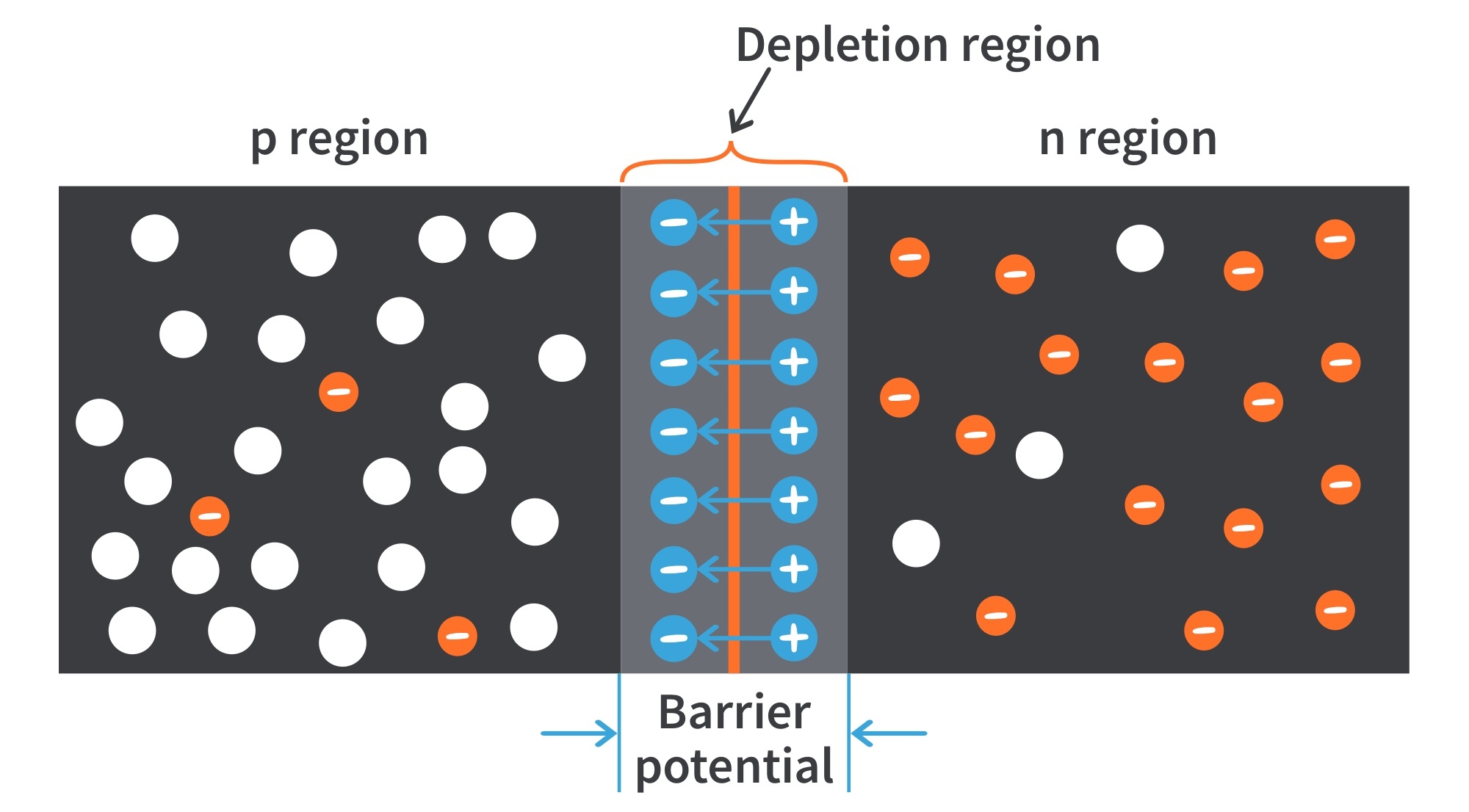
If a piece of intrinsic silicon is doped so that part is n-type and the other part is p-type, a pn junction forms at the boundary between the two regions and a diode is created, as in Fig. 12.
Figure 12: PN junction formation showing the majority and minority carriers.
The p region has many holes and a few thermally generated free electrons. The n region has many free electrons and a few thermally generated holes.
The PN Junction
Formation of the Depletion Region
Before the pn junction is formed, note that there are as many electrons as protons in the n-type or p-type material, making the material neutral.
At the instant of the pn junction formation, the free electrons near the junction in the n region begin to diffuse across the junction into the p region where they combine with holes near the junction, as shown in Fig 13.
Figure 13: Formation of the depletion region.
The n region loses free electrons as they diffuse across the junction, creating a layer of positive charges near the junction. Then the p region loses holes as the electrons and holes combine, creating a layer of negative charges near the junction.
The two layers of charges form the depletion region; the region near the pn junction depleted of carriers due to diffusion across the junction.
After the surge of electrons across the pn junction, the depletion region will expand to a point where the total negative charge in the depletion region repels diffusion of electrons into the p region and the diffusion stops.
The depletion region acts as a barrier to the further movement of electrons across the junction.
The PN Junction
Energy Diagrams of the PN Junction and Depletion Region
Trivalent impurities exert lower forces on the outer-shell electrons than the pentavalent impurities.
The lower forces in p-type materials mean that the electron orbits are slightly larger and hence have greater energy than the electron orbits in the n-type materials.
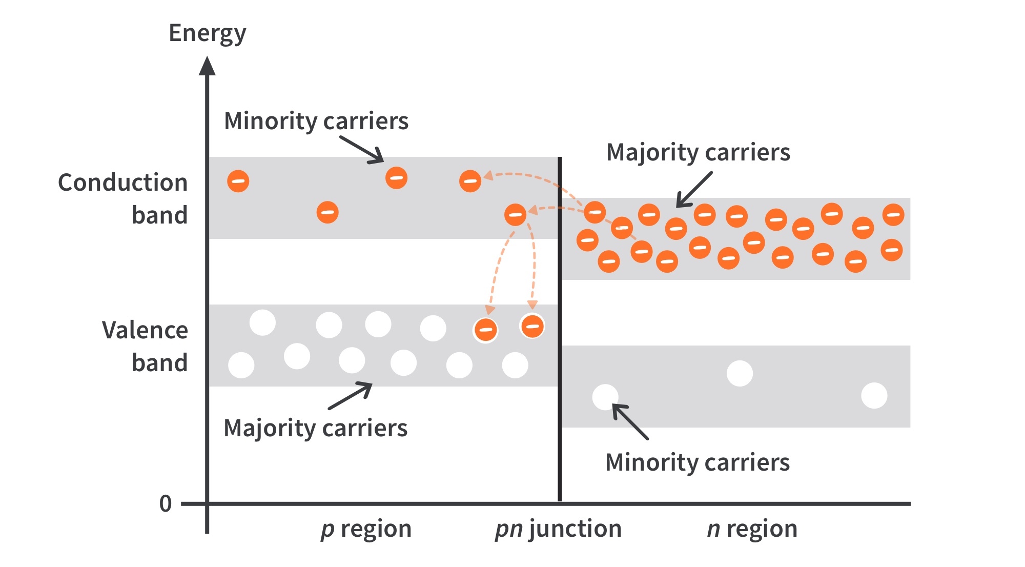
An energy diagram for a pn junction at the instant of formation is shown in Fig. 14.
Figure 14: Energy diagram at the instant of junction formation
The valence and conduction bands in the n region are at lower energy levels than those in the p region, but there is a significant amount of overlapping.
The free electrons in the n region in the upper part of the conduction band can easily diffuse across the junction (even with no energy gain) and temporarily become free electrons in the lower part of the p-region conduction band.
After crossing the junction, the electrons quickly lose energy and fall into the holes in the p-region valence band.
As diffusion continues, the depletion region forms and the energy level of the n-region conduction band decreases due to the loss of higher-energy electrons that have diffused to the p region.
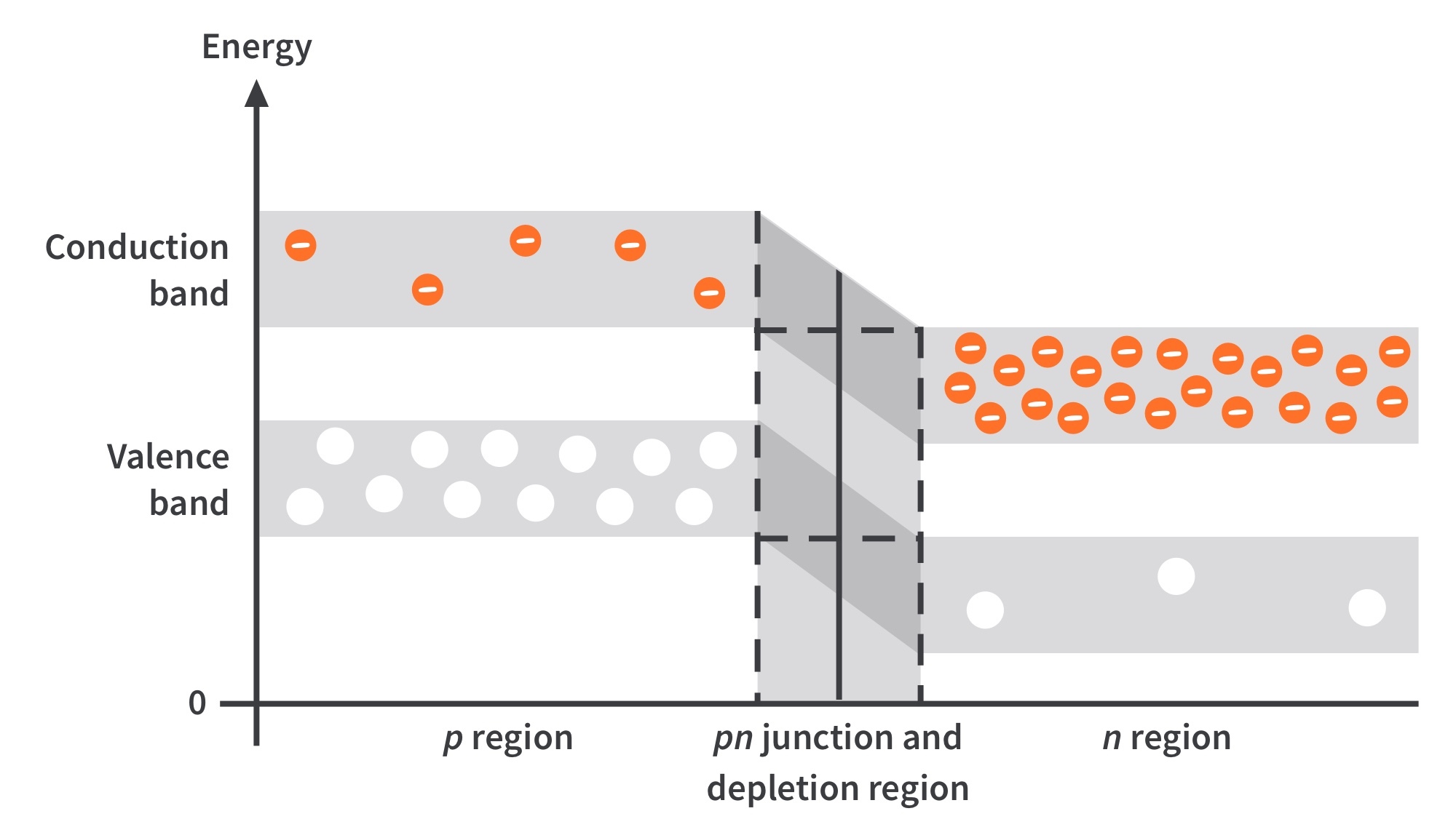
Soon, there are no electrons left in the n-region conduction band with enough energy to get across to the p-region, as indicated by the alignment of the top of the n-region and the bottom of the p-region conduction band in Fig. 15.
Figure 15: Energy diagram at equilibrium
At this point, the junction is at equilibrium; and the depletion region is complete because diffusion has ceased.
The energy gradient across the depletion region acts as an “energy hill” that an n-region electron must climb to get to the p region.
As the energy level of the n-region conduction band has shifted downward, the energy level of the valence band has also shifted downward.
It still takes the same amount of energy for a valence electron to become a free electron. The energy gap between the valence band and the conduction band remains the same.
The PN Junction
Barrier Potential
The potential difference of the electric field across the depletion region is the amount of voltage required to move electrons through the electric field. This potential difference is called the barrier potential, expressed in volts.
The barrier potential of a pn junction depends on several factors, including the type of semiconductive material, the amount of doping, and the temperature.
The typical barrier potential is approximately 0.7 V for silicon and 0.3 V for germanium at 25 oC.
Get the latest tools and tutorials, fresh from the toaster.