Bias establishes the DC operating point (Q-point) for proper linear operation of an amplifier.
If an amplifier is not biased with correct DC voltages on the input and output, it can go into saturation or cutoff when an input signal is applied.
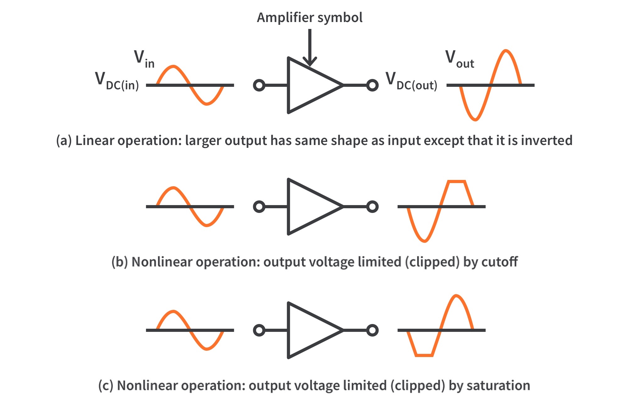
Figure 1: Examples of linear and nonlinear operation of an inverting amplifier
In Fig. 1(a), the output is an amplified replica of the input signal but inverted, which means that it is out of phase with the input. The output signal swings equally above and below the DC bias level of the output, VDC(out).
Fig. 1(b) and (c) illustrate the distortion in the output signal caused by improper biasing.
Fig. 1(b) shows the limiting of the positive portion of the output as a result of a Q-point being too close to cutoff. Fig.1(c) shows limiting of the negative portion of the output with a Q-point too close to saturation.
The DC Operating Point
Graphical Analysis
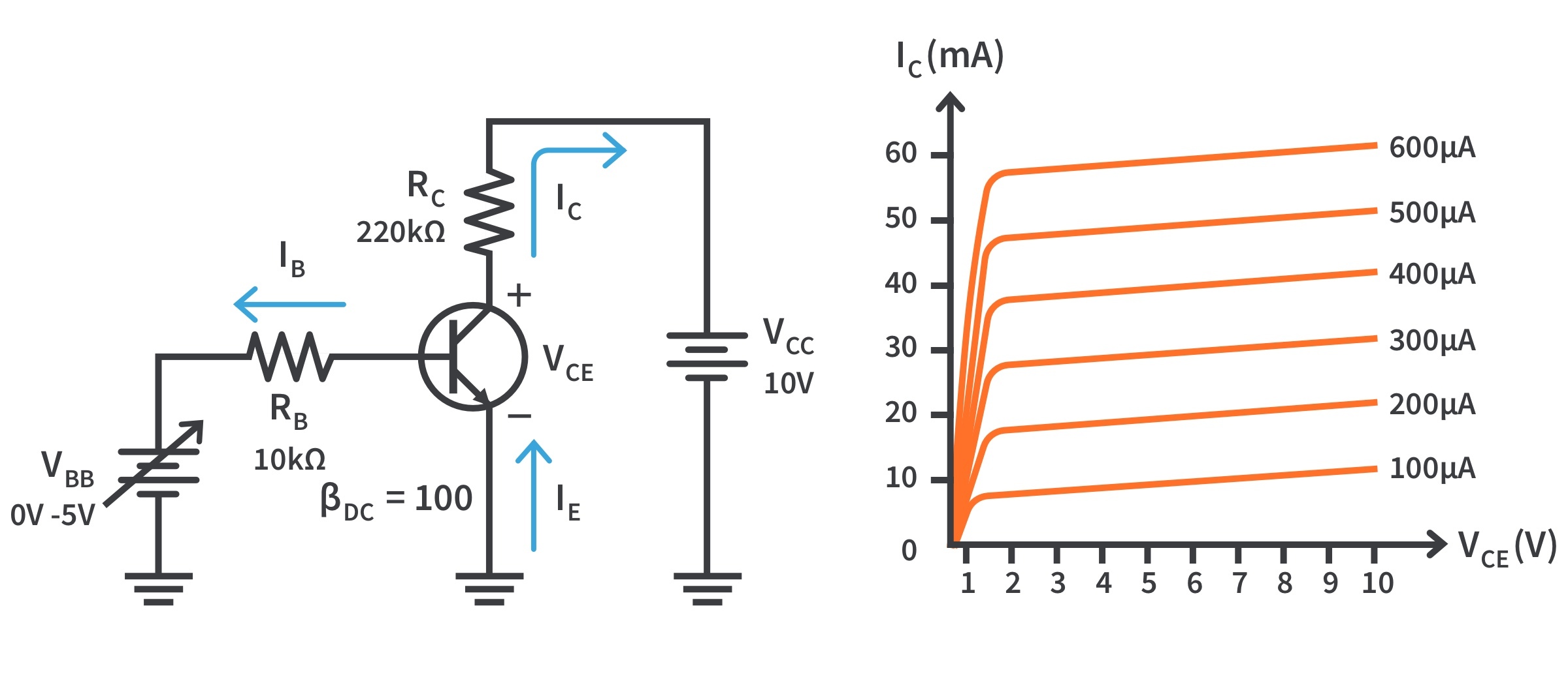
The transistor in Fig. 2(a) is biased with VCC and VBB to obtain certain values of IB, IC, IE, and VCE. The collector characteristic curves for this transistor are shown in Fig. 2(b); which graphically illustrate the effects of DC bias.
Figure 2: A DC-biased transistor circuit with variable bias voltage and the collector characteristic curves
We assign three values to IB and observe what happens to IC and VCE. First, VBB is adjusted to produce an IB of 200 A as shown in Fig. 3(a). Since IC =βDCIB, the collector current is 20 mA as indicated, and
This Q-point is shown on the graph of Fig. 3(a) as Q1.
Next, as shown in Fig. 3(b), VBB is increased to produce an IB of 300 A and an IC of 30 mA.
The Q-point for this condition is indicated by Q2on the graph.
Finally, VBB is increased to give an IB of 400 A and an IC of 40 mA.
Q3 is the corresponding Q-point on the graph in Fig. 3(c).
Figure 3: Illustration of Q-point adjustment
The DC Operating Point
DC Load Line
describes graphically the DC operation of a transistor circuit
a straight line drawn on the characteristic curves from the saturation value where IC = IC(sat) on the y-axis to the cutoff value where VCE = VCC on the x-axis, as shown in Fig. 4(a)
determined by the external circuit (VCC and RC), not the transistor itself
In Fig. 3, the equation for IC is
This is the equation of a straight line with a slope of -1/RC, an x intercept of VCE = VCC, and a y intercept of VCC/RC, which is IC(sat).
Figure 4: The DC load line
The point at which the load line intersects a characteristic curve represents the Q-point for that particular value of IB. Fig. 4(b) illustrates the Q-point on the load line for each value of IB in Fig. 3.
The DC Operating Point
Linear Operation
The region along the load line including all points between saturation and cutoff is the linear region of the transistor’s operation.
In this region, the output voltage is ideally a linear reproduction of the input.
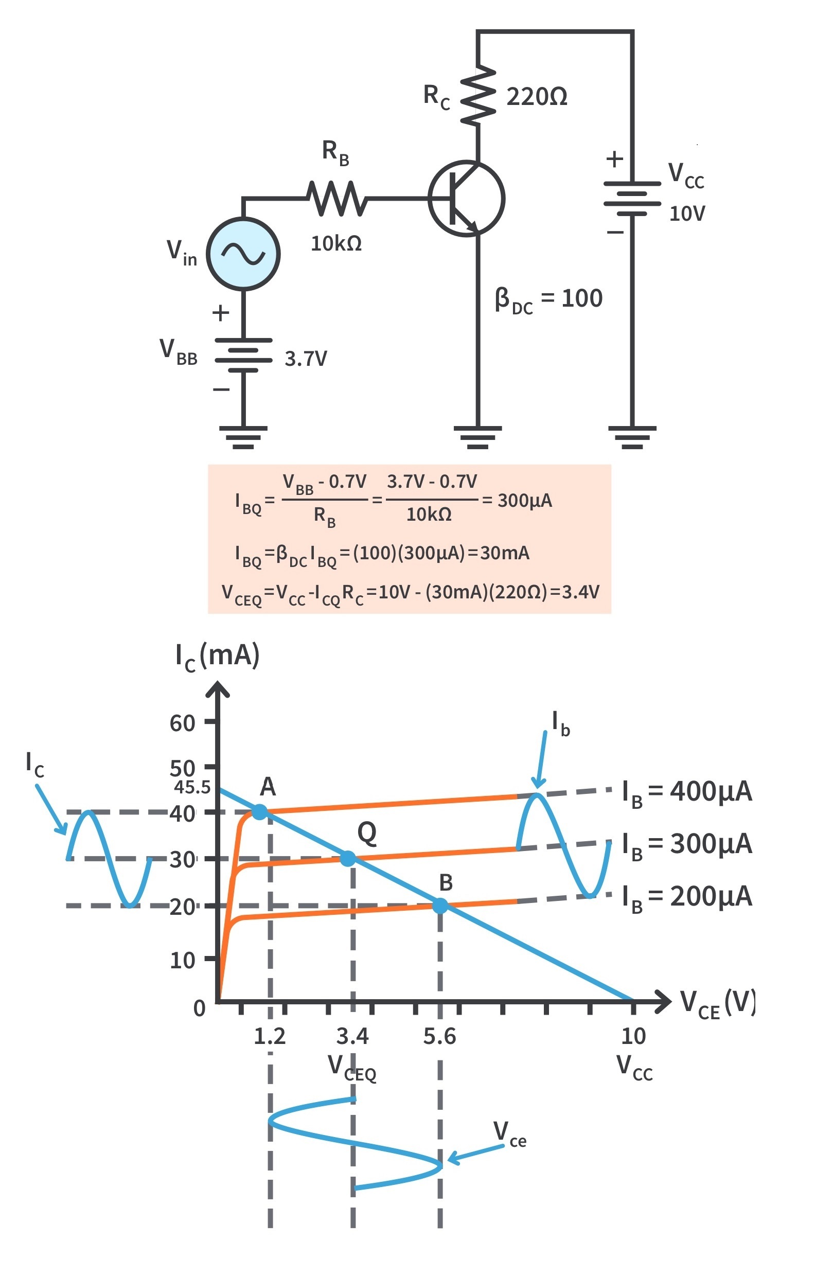
Figure 5 shows an example of the linear operation of a transistor. AC quantities are indicated by lowercase italic subscripts.
Figure 5: Variations in collector current and collector-to-emitter voltage as a result of a variation in base current.
A sinusoidal voltage, Vin, is superimposed on VBB, causing IB to vary sinusoidally above and below its Q-point value of 300 A. This causes IC to vary 10 mA above and below its Q-point value of 30 mA.
As a result of the variation IC, VCE varies 2.2 V above and below its Q-point value of 3.4 V.
Point A on the load line in Fig. 5 corresponds to the positive peak of the sinusoidal input voltage. Point B corresponds to the negative peak, and point Q corresponds to the zero value of the sine wave.
VCEQ, ICQ, and IBQ are DC Q-point values with no input sinusoidal voltage applied.
Voltage-Divider Bias
A more practical bias method is to use VCC as the single bias source, as shown in Fig. 6. To simplify the schematic, the battery symbol is omitted and replaced by a line termination circle with a voltage indicator (VCC).
Figure 6: Voltage-divider bias
A DC bias voltage at the base of the transistor can be developed by a resistive voltage divider that consists of R1 and R2. VCC is the DC collector supply voltage.
Since IB << I2, the voltage-divider circuit analysis is straightforward because the loading effect of IBcan be ignored (stiff voltage divider).
To analyze a voltage-divider circuit in which IB is small compared to I2, first calculate VB using the unloaded voltage-divider rule:
Once you know VB , you can find the voltages and currents in the circuit, as follows:
Once you know VC and VE, you can determine VCE.
If the input resistance is raised, the voltage divider may not be stiff; and more detailed analysis is required to calculate circuit parameters.
Voltage-Divider Bias
Loading Effects of Voltage-Divider Bias
The DC input resistance of the transistor is proportional to βDC so it will change for different transistors.
When a transistor is operating in its linear region, IE = βDCIB.
When the emitter resistor is viewed from the base circuit, the resistor appears to be larger than its actual value because of the DC current gain in the transistor. That is,
As long as RIN(BASE) is at least ten times larger than R2, the loading effect will be 10% or less and the voltage divider is considered stiff.
If RIN(BASE) is less than ten times R2, it should be combined in parallel with R2.
Thevenin’s Theorem Applied to Voltage-Divider Bias
To analyze a voltage-divider biased transistor circuit for base current loading effects, we will apply Thevenin’s theorem.
For the circuit in Fig. 7(a), looking out from the base terminal, the bias circuit can be redrawn as shown in Fig. 7(b).
Figure 7: Thevenizing the bias circuit
Apply Thevenin’s theorem to the circuit left of point A, with VCC replaced by a short to ground and the transistor disconnected from the circuit. The voltage at point A with respect to ground is
and the resistance is
The Thevenin equivalent of the bias circuit, connected to the transistor base, is shown in the box in Fig. 7(c). Applying Kirchhoff’s voltage law around the equivalent base-emitter loop gives
Using Ohm’s law, and solving for VTH,
Substituting IE/βDC for IB,
Solving for IE,
If RTH/βDC is small compared to RE, the result is the same as for an unloaded voltage divider.
Voltage-divider bias is widely used because reasonably good bias stability is achieved with a single supply voltage.
Other Bias Methods
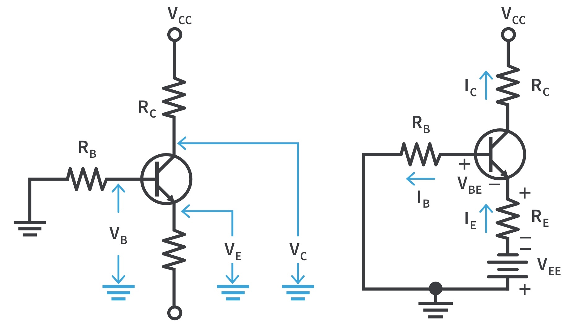
Emitter Bias
Emitter bias provides excellent bias stability in spite of changes in or temperature. It uses both a positive and a negative supply voltage.
In an NPN circuit shown in Fig. 8, the small IB causes VB to be slightly below ground. VE is one diode drop less than this.
Figure 8: An NPN transistor with emitter bias. Polarities are reversed for a PNP transistor. Single subscripts indicate voltages with respect to ground.
The combination of the small drop across RB and VBE forces the emitter to be at approximately -1 V. Using this approximation,
VEE is entered as a negative value in this equation.
You can apply the approximation that to calculate VC:
The approximation that VE ≈ -1 V is useful for troubleshooting to circumvent detailed calculations.
Kirchhoff’s voltage law can be applied to develop a more accurate formula for IE for detailed analysis.
Kirchhoff’s voltage law applied around the base-emitter circuit in Fig. 8(a), which has been redrawn in part (b) for analysis, gives:
Substituting IB ≈ IE /βDC,
Solving for IE,
Voltages with respect to ground are indicated by a single subscript. VE with respect to ground is
VB with respect to ground is
VC with respect to ground is
Other Bias Methods
Base Bias
This method of biasing is common in switching circuits. Fig. 9 shows a base-biased transistor.
Figure 9: Base bias
The analysis of this circuit for the linear region shows that it is directly dependent on βDC. Starting with Kirchhoff’s voltage law around the base circuit,
Substituting IBRB for VRB and solving for IB,
Kirchhoff’s voltage law applied around the collector circuit in Fig. 9 gives the equation: VCC - ICRC - VCE = 0. Solving for VCE,
Substituting the expression for IB into IC=βDCIB yields
Q-Point Stability of Base Bias
A variation in βDC causes IC, and as a result, VCE to change, thus changing the Q-point of the transistor; making the base bias circuit extremely beta-dependent and unpredictable.
βDC varies with temperature and IC. Also, there is a large spread of values from one transistor to another of the same type due to manufacturing variations. Thus, base bias is rarely used in linear circuits.
Other Bias Methods
Emitter-Feedback Bias
If an emitter resistor is added to a base-bias circuit, the result is emitter-feedback bias, as shown in Fig. 10.
Figure 10: Emitter-feedback bias
The idea is to help make base bias more predictable with negative feedback, which negates any attempted change in IC with an opposing change in VB.
If IC tries to increase, VE increases, causing an increase in VB because VB =VE+VBE. This increase in VB reduces the voltage across RB, thus reducing IB and keeping IC from increasing. A similar action occurs if IC tries to decrease.
To calculate IE, you can write Kirchhoff’s voltage law (KVL) around the base circuit.
Substituting IE/βDC for IB, IE is equal to
While emitter-feedback bias is better for linear circuits than base bias, it is still dependent on βDC and is not as predictable as voltage-divider bias.
Other Bias Methods
Collector-Feedback Bias
In Fig. 11, RB is connected to the collector rather than to VCC, as it was in the base bias arrangement. VC provides the bias for the base-emitter junction. The negative feedback creates an “offsetting” effect that keeps the Q-point stable.
Figure 11: Collector-feedback bias
If IC tries to increase, it drops more voltage across RC, thereby causing VC to decrease. When VC decreases, there is a decrease in voltage across RB, which decreases IB.
The decrease in IB produces less IC which, in turn, drops less voltage across RC and thus offsets the decrease in VC.
Analysis of a Collector-Feedback Bias Circuit
By Ohm’s law, IB can be expressed as
Assuming that IC >> IB, VC ≈ VCC - IC RC. Also, IB=IC /βDC . Substituting for VC in the equation IB=(VC-VBE)/RB,
Solving for IC ,
Since the emitter is ground, VCE=VC.
Q-Point Stability Over Temperature
IC is dependent to some extent on βDC and VBE. This dependency can be minimized by making RC >> RB/βDC and VCC>>VBE.
As the temperature goes up, βDC goes up and VBEgoes down. The increase in DC acts to increase IC. The decrease in VBEacts to increase IB which, in turn also acts to increase IC.
As IC tries to increase, VRC also tries to increase. This tends to reduce VC and therefore VRB, thus reducing IB and offsetting the attempted increase in IC and decrease in VC.
The result is that the collector-feedback circuit maintains a relatively stable Q-point. The reverse action occurs when the temperature decreases.
Get the latest tools and tutorials, fresh from the toaster.


 to calculate VC:


